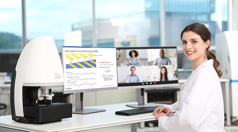

Reduces Cost and Increases Efficiency in Production of Semiconductor Wafers
Introduction
The scaling trend in semiconductor design requires tighter control over defects on wafers. In order to characterize the defects, both inspection and review tools are needed.
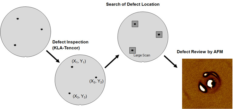
The inspection tools such as surface scanning inspection systems (SSIS) are employed first to locate and map defect sites, and the review tools such as scanning electron microscopy (SEM) are used to obtain morphological information.
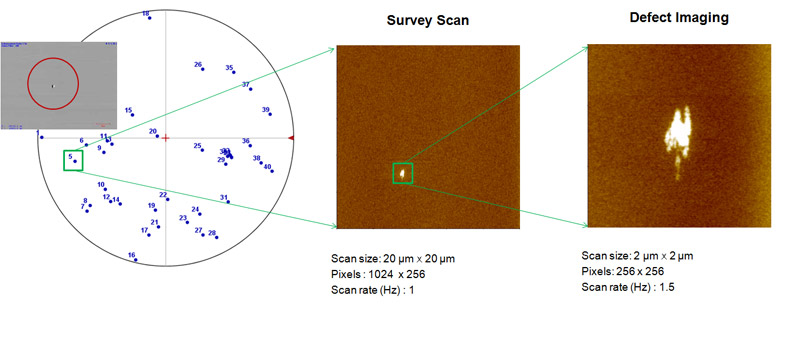
Large defects, which are visible by optical microscopy, can be easily found by an inspection tool and imaged by a review tool. However, as processing requirements become more stringent, the defect size of interest gets smaller, below the diffraction limit of optical microscopy. To locate and identify small defects, a large survey scan needs to be performed by the review tool in order to find the exact location of the defects.
Defect review SEM has been used to image the defects of a bare wafer after defect sites are mapped by the laser-scattering defect inspection tools such as Surfscan from KLATencor. However, the imaging by defect review SEM is limited to 2D and cannot provide the 3D information, which has become more crucial in recent days for bare wafer manufacturing control. Also, smaller defects, less than 50nm, are increasingly not detected by defect review SEM.
Why Automatic Defect Review (ADR) AFM?
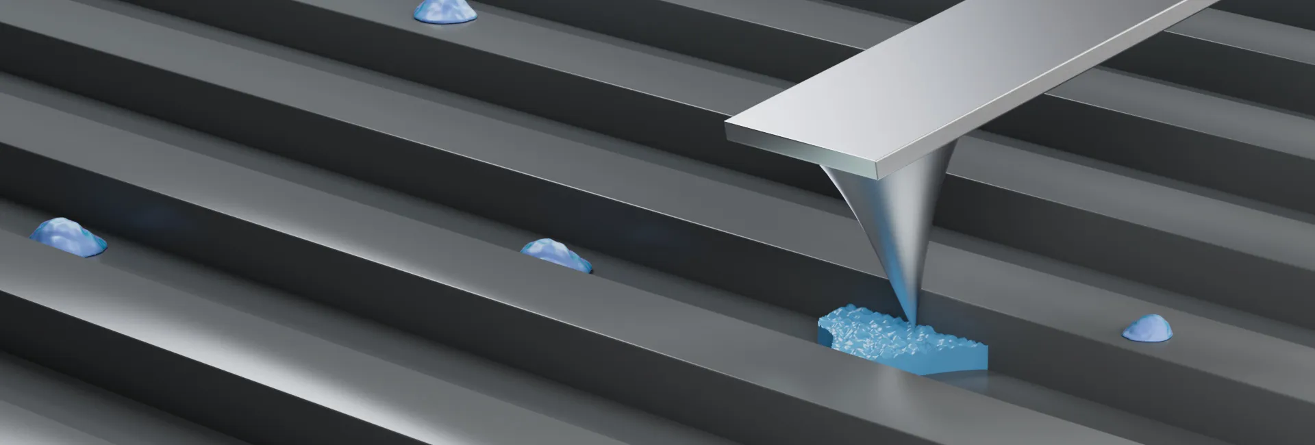
Atomic force microscopy (AFM) is gaining more importance as the choice of a review tool in recent days because it can directly measure the defect dimensions (height and width, hence shape) and the physical properties of defects of interest. However, for engineers and researchers working with bare wafers, the process of identifying nanoscale defects is time consuming with conventional manual AFM, hindering productivity, let alone throughput. Thus it is important to have an automated solution for both failure analysis and production engineers who need to find the cause of defect sites on bare wafers and minimize them.
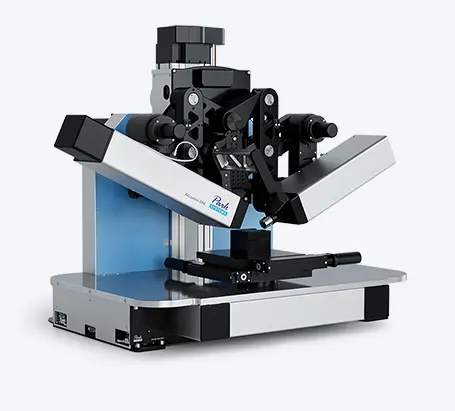
To address this need, Park Systems have delivered the Automatic Defect Review (ADR) AFM which speeds up and improves the way defects are imaged and analyzed. With this solution, users are now able to obtain the additional details and the height/depth information of the defects which were not possible or too expensive to obtain with SEM based ADR.
How to Transfer Defect Map from Inspection Tool to Review AFM
The general defect review concept is simple, yet complicated when it is done on the nanometer scale. Simple, because all it would require is the proper transferring of the defect map from an inspection tool and re-locating those same defects on a review tool. Coordinates from the inspection tool are translated to the review tool, which is used to zoom in and image the details of the defect, revealing its characteristics.
The complicated part comes into play when attempting to accurately go near the defect site, in order to image it, and to do this all in automation. This is due to the fact that there are stage mapping errors between the inspection tool and the review tool.
In case of a patterned wafer, alignment marks are used as reference points to map the two stages between the inspection tool and AFM, and the position error from both tools can be accurately estimated. Park’s initial success in Automated Defect Review (ADR) AFM solution was implemented in the hard disk industry, utilizing the reference marks inscribed by the optical inspection tool such as KLA Tencor’s Candela series. Utilizing these marks, the defect maps of hard disk media or substrates could be accurately and reliably transferred and the automated review AFM, Park HDM Series, was able to get near enough to the defect to conduct a survey scan, and then follow up with a zoom-in scan to provide the details the user required. As a whole, this solution proved to be effective, increasing the productivity in the HDD industry’s FA labs by up to 1000%.
Automated, Accurate Transfer of Defect Map WITHOUT Reference Marks
Success in the HDD industry resulted in similar requests coming from the semiconductor industry. Since the cleanness level requirement for the semiconductor industry is much stricter than that of HDD, creating markers on the bare wafers is not possible, hence the need for ADR process WITHOUT any reference marking on a bare wafer is required.
Without alignment marks the positions of defects are roughly estimated [1, 2]. Therefore, additional alignment process is required to decrease the positional error [3] during the defect map transfer. To address this issue, a new method was developed that utilizes the wafer edge, notch, and large defects, which are visible by optical microscopy, as the reference points.
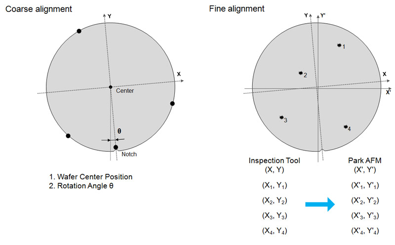
The improved remapping technique, combined with enhanced vision, does not require any reference marker on a bare wafer. Furthermore, it also does not need any separate step to calibrate the stage of the targeted inspection system.
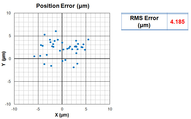
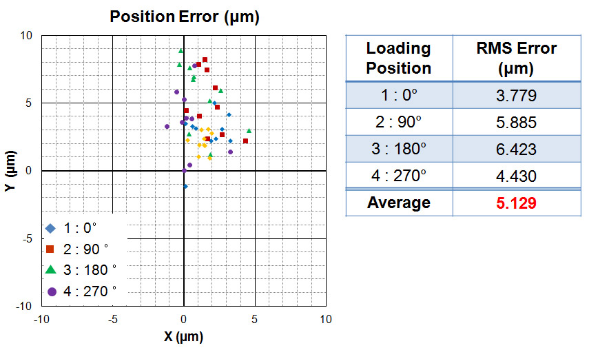
The success rate of the 300mm bare wafer ADR depends on two factors: the accuracy of stage mapping and the size of initial survey scan. The more accurate the stage mapping, the smaller survey scan size can be used for higher success in finding the defect. The new stage mapping technique vastly improves the accuracy by adopting advanced remapping algorithm and enhanced vision technique.
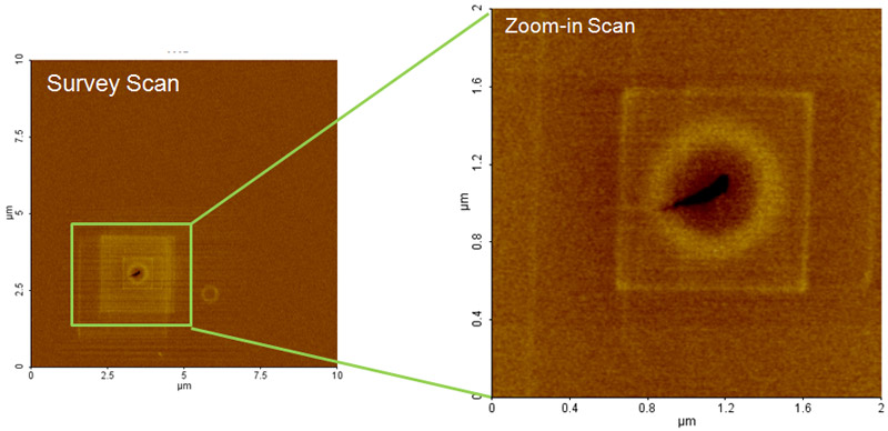
The RMS position error of survey scans are less than 5 μm regardless of wafer loading positions. It means that all the defects are located within ±5 μm using the defect map provided from a defect inspection tool.
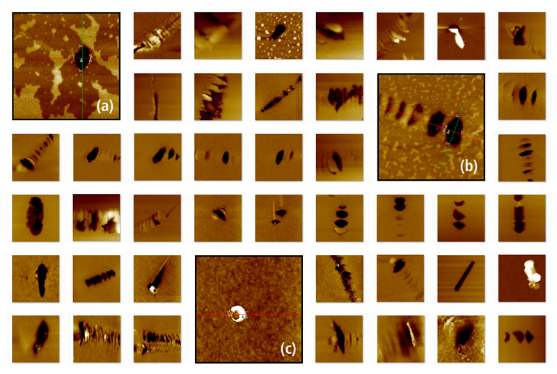
Conclusion: Results of 300 mm Bare Wafers ADR by Park NX-Wafer
Utilizing the advanced coordinate translation technique, the defect map obtained from a laser-scattering defect inspection tool, such as Surfscan from KLA-Tencor, can be accurately transferred to a 300mm AFM system, allowing full automation for high throughput defect imaging.
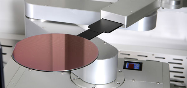
With the new 300mm bare wafer ADR, a typical automated measurement run would go as follows.
- A bare wafer is run by a laser-scattering defect inspection tool (e.g. Surfscan)
- Then an operator registers the resulting defect coordinates file, known as KLARF for the Surfscan tool, to Park NX-Wafer.
- The coordinates of the defect map are automatically de-skewed and the linkage of the two stages is enabled between the inspection tool and Park NX-Wafer
- Park NX-Wafer then runs the automatic defect review (ADR) on the sample bare wafer.
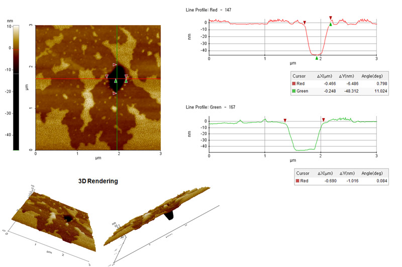
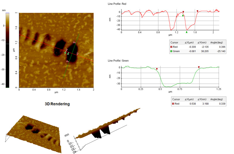
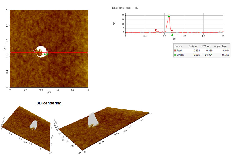
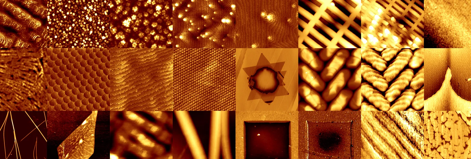
The above set of data shows the results from the 300mm bare wafer ADR with Park NX-Wafer. Typical success rate is higher than 95% regardless of the orientation of a wafer. The zoomed-in scans show the detailed morphology of defects, clearly distinguishing various types such as pit, bump, and scratch.