Ardavan Zandiatashbara*, Patrick A. Taylorb, Byong Kima, Young-kook Yooa, Keibock Leea, Ahjin Joc, Ju Suk Leec, Sang-Joon Choc, and Sang-il Parkc
a Park Systems Inc., 3040 Olcott St., Santa Clara, CA, USA 95054
b SunEdison Semiconductor, St Peters, MO, USA 63376
c Park Systems Corp., KANC 4F, Iui-Dong 906-10, Suwon, Korea 443-270
ABSTRACT
Single crystal silicon wafers are the fundamental elements of semiconductor manufacturing industry. The wafers produced by Czochralski (CZ) process are very high quality single crystalline materials with known defects that are formed during the crystal growth or modified by further processing. While defects can be unfavorable for yield for some manufactured electrical devices, a group of defects like oxide precipitates can have both positive and negative impacts on the final device. The spatial distribution of these defects may be found by scattering techniques. However, due to limitations of scattering (i.e. light wavelength), many crystal defects are either poorly classified or not detected. Therefore a high throughput and accurate characterization of their shape and dimension is essential for reviewing the defects and proper classification. While scanning electron microscopy (SEM) can provide high resolution twodimensional images, atomic force microscopy (AFM) is essential for obtaining three-dimensional information of the defects of interest (DOI) as it is known to provide the highest vertical resolution among all techniques [1]. However AFM's low throughput, limited tip life, and laborious efforts for locating the DOI have been the limitations of this technique for defect review for 300 mm wafers. To address these limitations of AFM, automatic defect review AFM has been introduced recently [2], and is utilized in this work for studying DOI on 300 mm silicon wafer. In this work, we carefully etched a 300 mm silicon wafer with a gaseous acid in a reducing atmosphere at a temperature and for a sufficient duration to decorate and grow the crystal defects to a size capable of being detected as light scattering defects [3]. The etched defects form a shallow structure and their distribution and relative size are inspected by laser light scattering (LLS). However, several groups of defects couldn't be properly sized by the LLS due to the very shallow depth and low light scattering. Likewise, SEM cannot be used effectively for post-inspection defect review and classification of these very shallow types of defects. To verify and obtain accurate shape and three-dimensional information of those defects, automatic defect review AFM (ADR AFM) is utilized for accurate locating and imaging of DOI. In ADR AFM, non-contact mode imaging is used for non-destructive characterization and preserving tip sharpness for data repeatability and reproducibility. Locating DOI and imaging are performed automatically with a throughput of many defects per hour. Topography images of DOI has been collected and compared with SEM images. The ADR AFM has been shown as a non-destructive metrology tool for defect review and obtaining three-dimensional topography information.
Keywords: Atomic force microscopy, defect review, defect classification, defect inspection, non-contact mode, failure analysis, automated AFM, metrology.
1. MOTIVATION
As integrated devices continue to shrink, incoming bare silicon wafer defectivity requirements become more and more stringent. The inspection of bare silicon wafers for surface defects is predominantly accomplished by measuring the difference in laser light scattering (LLS) between the clean surface and a surface defect, where the intensity of the scattered signal is compared to the LLS of a standard latex sphere. The actual surface defectivity can originate from added particles, topological defects, and crystal imperfections. To be able to reduce the number of defects one must know the source of the defect. LLS inspection can only give defectivity counts and a relative size. Therefore, one must rely on defect review techniques such as SEM and AFM to determine the nature and origin of the defects. In this study we focus on very small crystal imperfections which are not easily observed by LLS without some means to make them larger. We have used a decorative etching technique to highlight crystal imperfections to be studied by LLS, SEM, and AFM. The defect analysis can only be accomplished with accurate and reproducible defect coordinate transfer between analysis tools. Here we show how we have successfully and reliably found and characterized the decorated defects by AFM.
2. ADR AFM PROCEDURE
The process in ADR AFM is depicted in figure 1. During this process, the defects of interest are located accurately and imaged non-destructively. Two factors are essential in order to achieve these objectives. First proper linkage between ADR AFM and LLS inspection tool is required to minimize the positioning errors and locate the defects accurately. The linkage for blank wafers is achieved by sample coordinate alignment. Generally there are no alignment markers or fiducials available on blank wafers to be used for alignment. Therefore ADR AFM uses specialized vision to perform the sample alignment properly. Another important factor in AFM defect review is non-contact mode imaging which is required for non-destructive imaging of the samples while preserving AFM tip life such that the tip can last throughout the process for multiple defects.
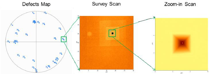 Figure 1.
The schematic shows ADR AFM process for this study. After completing coordinate mapping, ADR AFM will automatically perform survey scan, zoom-in scan, processing, analysis, and classification for each defect.
2.1 Coordinate alignment
Sample coordinate alignment is needed for proper linkage between the stage coordinates of ADR AFM and LLS inspection tool. In the case of blank wafers, no fiducial or alignment marker exists on the sample to be used for sample alignment. To overcome this challenge, a coarse alignment followed by a fine alignment is performed. In the coarse alignment, three randomly selected peripheral and the notch or an angular reference are selected to correct for translational and rotational errors. This is followed by a fine alignment to eliminate positioning errors due to non-affinity between the stage coordinates of ADR AFM and LLS inspection tool. A few large defects with known inspection coordinates are used for performing fine alignment. Since the defects are hardly visible in a standard AFM optical image, an enhanced vision is used to locate the defects in the optics of the ADR AFM and utilize the defects as aligner markers. Upon the sample alignment, ADR AFM is able to locate additional defects accurately. More details on coordinate alignment can be found in ref [2].
2.2 Enhanced vision
Enhanced vision is utilized during fine coordinate alignment to locate the defects in the optical vision of ADR AFM. The technique is developed based on well-known differential frame averaging of the optical frames collected from the sample surface at two accurately separated locations. The sample can be moved accurately since ADR AFM uses a separated Z and XY scanners configuration. This architecture was initially developed to eliminate the crosstalk between the XY and Z scanners (which has been a common artifact in tube scanner based AFM systems) [2]. In this setup, sample is moved by XY scanner while tip is following the sample topography by Z scanner. In enhanced vision, the optical frames of the sample are collected at two precisely separated locations, and then the final frame is generated from the difference between the collected frames. The resulting frame possesses an enhanced contrast of surface details which are not easily observable in the standard vision of ADR AFM. A comparison between the frames collected by standard vision versus enhanced vision is depicted in figure 2.
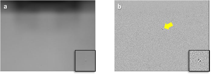 Figure 2.
a) Standard vs. b) enhanced vision images of a small defect on the surface of a bare silicon wafer are shown. The insets show a magnified view of the defect. The small defect is easily observable in enhanced vision. The larger image dimensions are 550 μm × 413 μm.
2.3 Non-contact mode imaging
Non-contact mode is the standard imaging mode in ADR AFM. It is essential to maintain tip sharpness during the defect review process from the first to the last defect that is located and imaged. In addition to keeping tip costs low, wellmaintained tip sharpness ensures consistent image quality and accuracy between the images of all defects during the process. It therefore enables the automated system to uninterruptedly locate and image the defects with a high throughput. In order to perform non-contact mode imaging, the AFM cantilever is oscillated at its resonance frequency. The oscillating cantilever is brought close enough to the sample that the oscillation amplitude reduces to a pre-defined setpoint due to the van der Waals tip sample interaction. ADR AFM maintains the oscillation amplitude to avoid tip contacting the sample. As the tip scans the sample surface, the oscillation amplitude is maintained by moving the cantilever up and down with the Z scanner to maintain its tip sample interaction in attractive regime. More details on non-contact mode imaging can be found in reference [4]. Although ADR AFM's functionality is based on non-contact mode imaging, it is capable of performing in other dynamic or contact imaging modes if needed.
2.4 Automatic defect search and imaging
The significant improvements in throughput of defect review are obtained by ADR AFM due to its fully automated process. Once defect coordinates from LLS inspection tool are entered into ADR AFM, coordinate alignment is performed, the defect is located and imaging starts for the list of selected defects. The process of locating and imaging the defects is fully automated. The automation includes locating the defect, tip-sample engagement, non-contact mode parameter optimization, survey scan, optimizing the scan size, final scan, processing, and defect classification. Defects 4 can be classified into two groups of bumps and pits. Defects are typically located within ±10 μm of their LLS coordinates.
3. SAMPLE PREPARATION (ETCHING PROCESS)
Bare 300mm diameter CZ silicon wafers were treated with a gaseous acid in a reducing atmosphere at a temperature and for a sufficient duration to grow the crystal imperfections [3]. The size and shape of the decorated defects depends on the nature of the original defect as shown in figure 3. Once decorated, the defect size is capable of being detected as LLS event. The LLS inspection tool locates and sizes the LLS events, providing the coordinates to be used by the SEM and AFM.
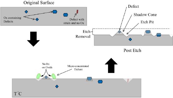 Figure 3.
Schematic of the process used to decorate crystal imperfections for defect inspection.
4. RESULTS
A wafer containing surface decorated defects was inspected by a LLS tool and 34 defects were selected to be reviewed by ADR AFM. The coordinates of the defects were entered to ADR AFM, coordinate alignment performed, and the defects were located and imaged by ADR AFM. The first 21 defects had been imaged by SEM before being studied by ADR AFM. However, SEM images only provide aerial two-dimensional view of defects without sufficient information on the defects depth and out of plane dimensions. The remaining 13 defects were not found by SEM despite the signal collected by the LLS tool. The summarized results of decorated defect study with ADR AFM and comparison with SEM results are demonstrated in figure 4. ADR AFM was able to find all the 34 defects including those that had not been found by SEM.
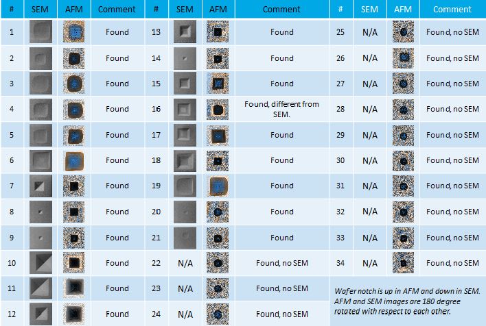 Figure 4.
The results of defect review with ADR AFM and comparison with SEM are shown. ADR AFM was able to locate
and image all the 34 defects.
The defects selected to be reviewed by ADR AFM belong to eight types according to their LLS signal. The tentative classification by the LLS tool is based on the defect's light scattering which is dependent on morphology, depth, and presenece of a central defect. As the decorative etching process proceeds, crystal imperfections are exposed and etch at a different rate than the perfect crystal surface. Defects exposed at the initial stages of the etch are deeper and more developed than defects exposed late in the etching proccess. Defects with an inverted pyramid shape are generally deeper and posses higher LLS signal. They are classified as "Facet". Defects with curved shape formed during the late stages of etching are shallower. These defects are classified as "Shallow". Some defects are exposed at an intermediate point in the decorative etch and have some degree of faceted walls with curved bottom. This category is classfied as "Both". Defects which have only started to be decorated have a very weak LLS signal and are classified as "Too shallow". The defects are also categorized whether or not they have the center defect, hence, a total of eight defect types were identified. The defect classification is tabulated in figure 5.
As we go from left to right side of the table in figure 5, the LLS signal become weaker. This was attributed to the depth of defects and the sharpness of the defect's edges. AFM images confirmed the depth difference between different classes of defects. Since the AFM images contain Z heights, we were able to use a banded color scale to depict the surface topography of the defects more accurately in 2D view.
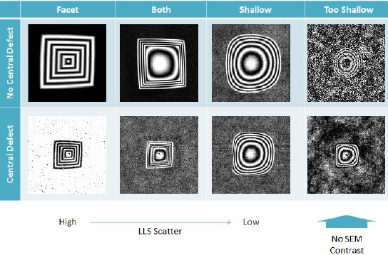 Figure 5.
Defect classification based on the LLS, SEM and AFM data .
5. DISCUSSION
Figure 6 depicts a comparison between the data collected with SEM vs. AFM for the same defect. Primary SEM image provides an aerial 2D view of the defect. However, the shallow depth of the defect reaches the limitations of SEM, hence, poor contrast in the image. As indicated in figure 5, shallower defects were not found by SEM. A secondary electron image helps identify the center defect. Identification of center defect by secondary electron is possible only if the defect was found in primary SEM image.
On the other hand, AFM image not only provides an aerial view of the defect, it also contains the height/depth values for each pixel. Therefore, more information can be obtained about the true topology of the defect by using a 3D representation of the AFM image or using a contoured color scale. Contoured color scales can also help understanding the topology of the defect in aerial view as shown in figure 5. As indicated before, AFM has the highest vertical resolution among all imaging techniques [1], hence, better contrast of AFM images in aerial view.
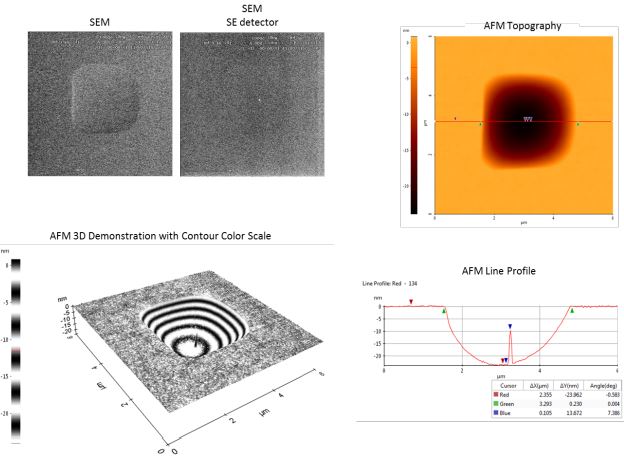 Figure 6.
Comparison between the data collected with SEM versus AFM. SEM image provides an aerial 2D view of the defect. Secondary electron image indicates the presence of center defect. AFM image, in addition to aerial 2D view, includes the 3D data. Therefore a line profile, 3D demonstration, and contoured color scale can be utilized to obtain more information.
All of the 34 defects were found by ADR AFM including the 13 defects that were not found by SEM. Figure 7 depicts the AFM images a defect that was not found by SEM. The defect depth is below 4 nm and contains a center defect. This example indicates once again the limitation of SEM resolution in out of plane direction.
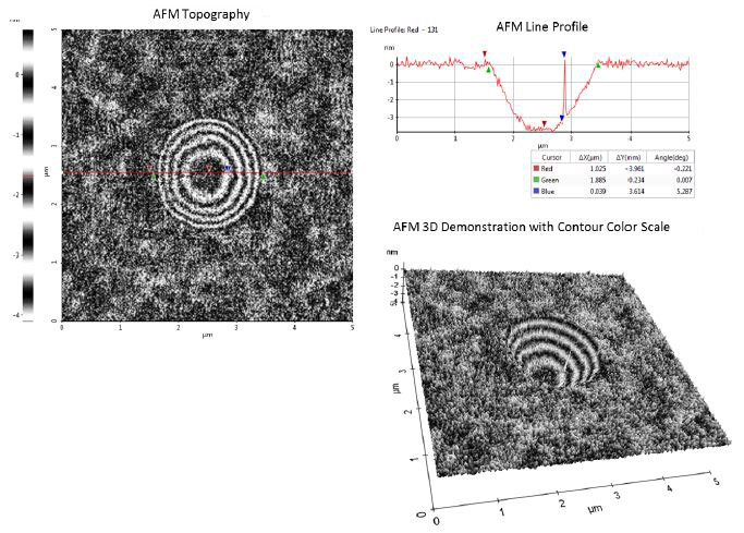 Figure 7.
AFM data for defect #24, which was not found by SEM.
It was indicated above that ADR AFM is a non-destructive imaging technique. It utilizes non-contact mode imaging for survey scan and final imaging scan. However, SEM beam can still modify the sample surface. Figure 8 indicates the sample contamination as a result of electron beam "burning" the surface during SEM imaging. These SEM burn-mark sizes are related to the SEM magnification. Figure 8 shows that several SEM magnifications were used in analyzing this defect.
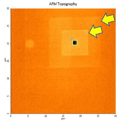
Figure 8.
AFM of a Facet defect with several SEM burn-marks.
6. SUMMARY
We have demonstrated the power of the ADR AFM to provide quality 3D information for defect review on bare silicon wafers. With the automated ADR AFM this type of analysis is simple and yet powerful.
REFERENCES
[1] G. T. Smith, Industrial Metrology: Surfaces and Roundness.: Springer, 2002.
[2] Ardavan Zandiatashbar et al., "High-throughput automatic defect review for 300mm blank wafers with atomic force microscope," in Proc. SPIE 9424, Metrology, Inspection, and Process Control for Microlithography XXIX, 2015, p. 94241X.
[3] J. Libert and L. Fei, Method to Delineate Crystal Related Defects.: PCT Publication, WO2013055368(A1).
[4] Ardavan Zandiatashbar, "Sub-angstrom roughness repeatability with tip-to-tip correlation," NanoScientific, no. Winter, pp. 14-16, 2014.
[5] Ajay Kumar and Banqiue Wu, "Extreme Ultraviolet Lithography: A Review," Journal of Vacuum Science & Technology B, pp. 1743 - 1761, 2007.
[6] James A. Folta, J. Courtney Davidson , Cindy C. Larson, Christopher C. Walton, and Patrick A. Kearney, "Advances in low-defect multilayers for EUVL mask blanks," in Proceedings of SPIE 4688, Emerging Lithographic Technologies VI, 173, 2002.