
 The live demos are a great way for us to offer education on Park Atomic Force Microscopy Imaging to further enhance the user experience on our equipment." Keibock Lee, Park Systems President.
Santa Clara, CA September 10, 2014
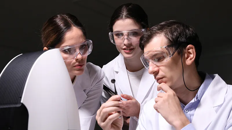
Park Systems, a leading manufacturer of atomic force microscopy (AFM) products will be hosting a series of live demonstrations via the internet of groundbreaking techniques widely used throughout many science and engineering disciplines. The next Live Demo will be on September 25 and will demonstrate how to do AFM Surface Roughness Measurements. To learn more go to http://www.parkafm.com/index.php/medias/events/live-demo.
"The live demos are a great way for us to offer education and instruction on Atomic Force Microscopy used in scientific research and engineering applications at nanoscale to a wide audience," commented Keibock Lee, Park Systems President. "We hope to use our live demos to create interactive nano science forums to exchange information and enhance user experiences on our AFM equipment."
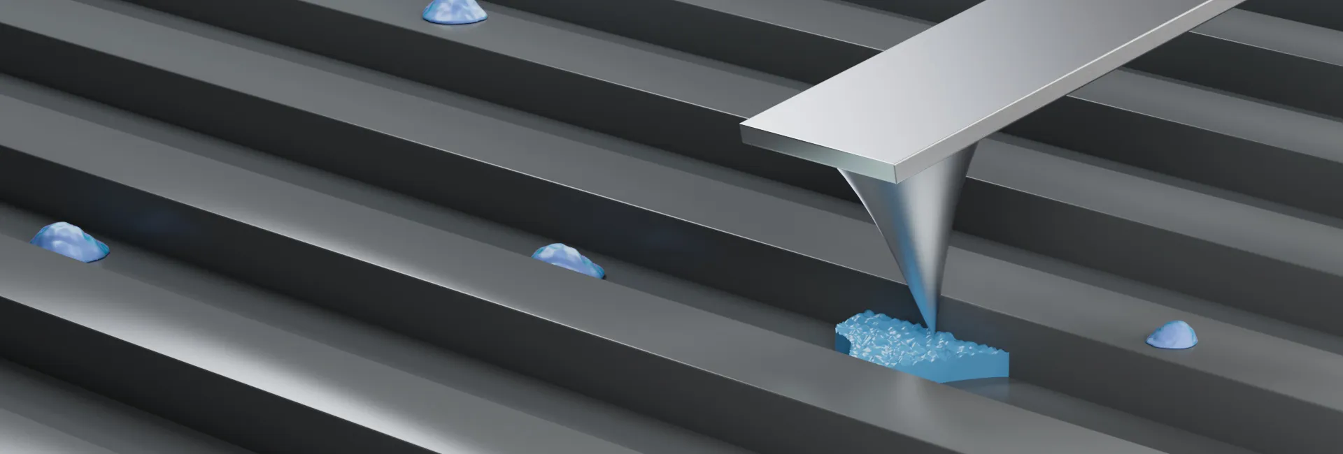
The live Demo on Sept 25 will demonstrate how to conduct Surface Roughness Measurement with AFM: Using non-contact mode imaging for angstrom level roughness measurement, one of the leading uses for AFM across many industries including Semiconductor Manufacturing where Automatic Defect Review drastically increases production yields and improves reliability.
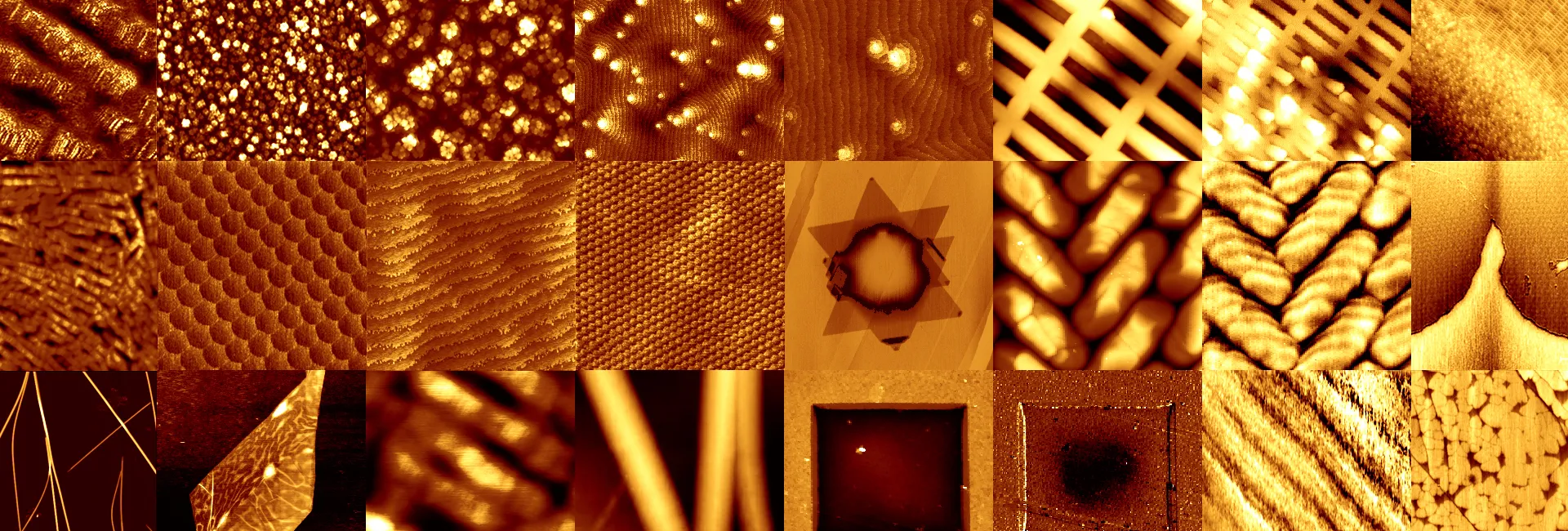
"Characterization of surface roughness for different materials is known to be one of the most common applications of scanning probe microscopy both in research and production," comments Park Systems Research Engineer and presenter Ardavan Zandiatashbar. "For example, both nanometer scale roughness of silicon wafers and surface quality after chemo-mechanical polishing are both key factors for successful semiconductor manufacturing."
Accurate, reliable and fast defect identification improves yield and ensure quality. Park AFM provides the only fully automated defect review process that improves reliability and throughput by 1,000%.
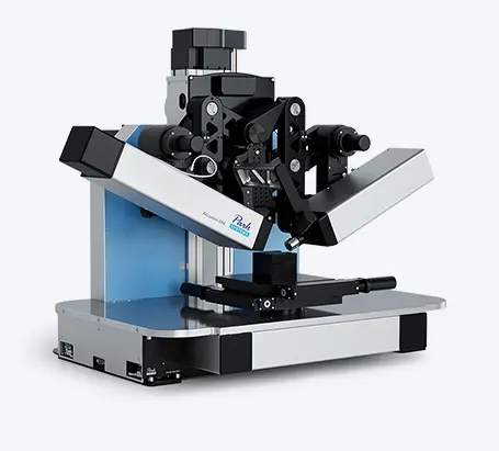
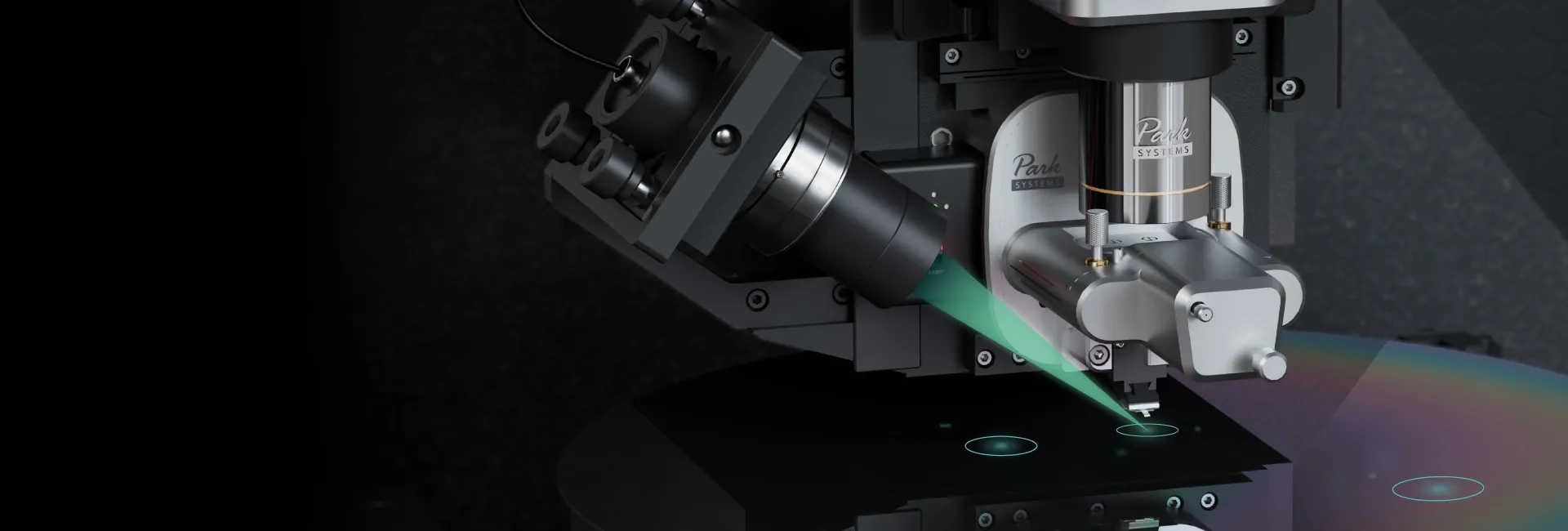
During this presentation, Park will demonstrate measurement of surface roughness using non-contact mode on bare silicon wafer using its new NX system, including how to change cantilevers, set up the tip and sample, and perform true non-contact mode imaging.
High Quality Liquid AFM Imaging LIVE DEMO
The first live demo, presented by Dr. Cynthia Buenviaje-Coggins and Dr. Byong Kim, Research Scientists at the Applications Laboratory, Park Systems Inc. was a demonstration on how to use Park Systems Atomic Force Microscope for reliable and accurate AFM measurements on a specific particle in liquid.
"Imaging and measuring size and elasticity of nanoparticles under wet conditions are important because nanoparticles are used in various applications such as vehicles in drug delivery and additives in cosmetics and paints," explains Dr. Cynthia Buenviaje-Coggins, Park Systems Research Scientist. "Conventional techniques allow for average size measurements but individual size and elasticity measurements on a specific particle in liquid would be challenging without the use of atomic force microscopy."
"In this presentation, we demonstrate how to take topographic images in liquid and force spectroscopy measurements on the samples comprised of Silica nanoparticles on Mica using AFM," commented Dr. Byong Kim, Research Scientist Park Systems. "During the demo, we change cantilevers, set up samples, and demonstrate tip approach into a liquid environment for liquid imaging. Using image analysis software, we show how to determine the size of the particles from the acquired AFM topography images. We also perform force spectroscopy measurements on and off the nanoparticle to determine differences between loading and unloading curves on the different areas. These differences correlate to characteristic elastic properties of those materials measured under wet conditions."
Park Systems offers a complete line of Atomic Force Microscopes for use in virtually every Nano Technology application from semiconductor to life science, from research to manufacturing and offers a range of products specifically designed to meet the needs each industry. For more information about Park Systems AFM, go to http://www.parkafm.com.
About Park Systems
Park Systems is a world-leading manufacturer of atomic force microscopy (AFM) systems with a complete range of products for researchers and industry engineers in chemistry, materials, physics, life sciences, semiconductor and data storage industries. Park's products are used by over a thousand institutions and corporations worldwide. Park's AFM provides highest data accuracy at nanoscale resolution, superior productivity, and lowest operating cost thanks to its unique technology and innovative engineering. Park Systems, Inc. is headquartered in Santa Clara, California with its global manufacturing, and R&D headquarters in Korea. Park's products are sold and supported worldwide with regional headquarters in the US, Korea, Japan, and Singapore, and distribution partners throughout Europe, Asia, and America. Please visit http://www.parkafm.com or call 408-986-1110 for more information.