


Advantages of High Vacuum for Electrical Scanning Probe Microscopy
Jonathan Ludwig1,2, Marco Mascaro1,2, Umberto Celano1, Wilfried Vandervorst1,2, Kristof Paredis1
1. IMEC, Leuven, Belgium
2. Department of Physics and Astronomy, University of Leuven, Leuven, Belgium.
Introduction
The discovery of graphene as the prototype of a new class of materials in 2004 has led to an enormous scientific interest in two-dimensional (2D) layered materials.1 Since then, a wide variety of 2D materials has been synthesized and explored.2-6Among them, the family of transition metal dichalcogenides (TMDs) has attracted specific interest from the semiconductor industry owing to an inherent band gap, a small dielectric constant, high mobilities, and ultrathinmaterials, which are heralded as promising candidates for scaling logic technology beyond the 5nm node. However, the integration of such materials in a 300mm compatible manufacturing environment still faces many challenges. As the praised properties have mostly been observed very locally, in flakes or single grains, the controlled growth, transfer and processing of high quality TMD layers remain a key hurdle.
Scanning probe microscopy, as an inherent high resolution 3D technique, is a powerful enabler for investigating the morphological and electrical properties of TMDs. In this technical note, we will illustrate the advantages of high vacuum for electrical measurements utilizing the capabilities of the Park NX-Hivacatomic force microscopy system (Park Systems) using MoS2 as an example material.
MoS2
A series of MoS2 samples with varying layer thickness were grown by metal organic chemical vapor deposition (MO-CVD) on sapphire substrates. All measurements are performed on the as-grown, un-transferred MoS2/sapphire. The room temperature mobility for devices made from the same material are found to be up to μm ~ 30 cm2/Vs, with higher average mobilities for thicker samples.12
Atomic force microscopy (AFM) images of all the samples measured are shown in figure 1. In total, three samples were measured with layer thicknesses of 1-2 layers, 3-4 layers, and one with pyramid structures, referred to here as multi-layered MoS2. The 1-2 layer sample consists of a completely closed monolayer MoS2 film with additional monolayer islands forming on top. These monolayer islands constitute the beginning of the growth of the second layer and can be identified as the light-colored regions in the topography image. Similarly, the 3-4 layer sample consists of a completely closed tri-layer MoS2 film with additional monolayer islands. An example of the sample structure for the 3-4 layer sample is shown in figure 1(d). Here, each green layer represents one layer of MoS2. In addition to MoS2 islands, we also see diagonal lines running across each sample. These are terraces from the sapphire substrate, which can be seen through the 2D film. The sapphire terraces can be unambiguously distinguished from MoS2 layers by the step height, 0.2nm for c-plane sapphires. 0.6nm for a monolayer MoS2 step, as can be seen from the cross section in figure 1 (f).13,14 The multi-layer sample differs from the other two in that the MoS2 surface is characterized by 3D pyramid-like structures. These pyramids sit on a completely closed tri-layer, and their formation is due to a change in the growth mechanism from layer-by-layer to 3D with increasing layer thickness. Details of the growth can be found in ref.12.
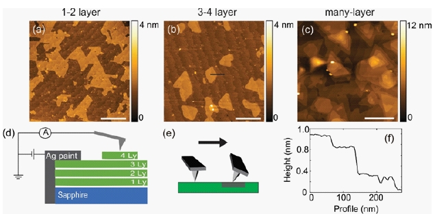
Fig. 1. (a-c) AFM topography images of the samples studied.
(d) Schematic of C-AFM setup used to measure multilayer MoS2 on a
sapphire. (e) Cartoon showing how the cantilever twists as it scans over
a high friction region. (f) Cross section of topography corresponding to
black line in (b) showing 0.6 nm step at the MoS2 island edge and
0.2nm step at the sapphire terrace. All images are plotted in Gwyddion.
Scale bar is 500 nm.
Conducting Scanning Probe Microscopy
Here we employ two conducting scanning probe microscopy (SPM) techniques to characterize the electronic properties of MoS2: Conductive Atomic Force Microscopy (C-AFM) and Scanning Tunneling Microscopy (STM). In C-AFM, the cantilever is in contact with the surface of the material and we simultaneously record topography and current. To measure the electrical current, a bias is applied to the sample chuck and current is measured by an external current amplifier connected to a conducting AFM probe. Electrical contact to the material is made by applying silver paint to the top and sides of the material. We use commercially available Pt-Ir coated probes, such as PPP-CONTSCPt or PPP-NCSTPt, with nominal spring constants in the range of 0.2 to 7 N/m. Since C-AFM is a contact-based AFM technique, it also allows the lateral force to be recorded along with the other C-AFM channels. Lateral force microscopy (LFM) measures the lateral deflection of the laser on the PSD due to torsion, or twisting, of the cantilever as it scans across the surface, as depicted in figure 1(e). The difference between the forward and reverse LFM images is proportional to the friction of the materialist differs from C-AFM in that a conductive wire, cut Pt-Ir in our case, is used to measure the tunneling current between the probe and the sample when the probe is a few angstroms above the surface. STM can be performed by either keeping the height constant and recording the current (referred to as constant height mode) or using the feedback to keep the current level constant and recording the height (constant current mode). In constant current mode, the height image contains both topographic and electronic information.
C-AFM in Air vs High Vacuum
In order to demonstrate the importance of the water layer on the surface on 2D materials, we performed C-AFM on the same MoS2 sample in air and high vacuum (HV), figure 2 (a-b) and (c-d), respectively. While the topography images for the scan in airand HVare quite similar, the C-AFM images differ considerably. Most notably, the measured current increases by three orders of magnitude in HV. The average current level in air is 1.4 nA at 5 V bias, while in HV it is 1.1 μA. The increase in current level is due to the removal of the thin water layer that is always present on the surface of the sample in air. This water layer is particularly problematic for MoS2 as it p-dopes the material, effectively turning it off electrically. From electrical transport of similar CVD grown MoS2 devices, the on state current is severely degraded and mobility decreases by 40% after exposure to DI water for two hours.15
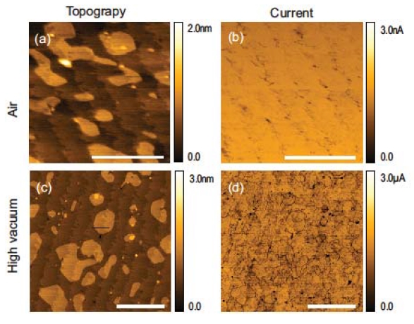
Fig. 2. C-AFM from the same 3-4 MoS2 sample showing the increased
current level and sensitivity under high vacuum. (a) Topography and (b)
current images in air at 5 V bias. (c) Topography and (d) current images
taken immediately after pumping to high vacuum at 0.5 V bias.
The data taken in air and high vacuum was acquired using identical
parameters: same probe with spring constant k of 7 N/m, set point of
10 nN, and 1 Hz scan rate. Scale bar is 500 nm.
Besides just an increase in current, the C-AFM image in HV shows much more detail. From the image in air, it appears that current is relatively homogeneous. Other than the current level, not much information can be extracted for the C-AFM in air on this sample. From the current map taken in HV, in contrast, we can clearly see the grain boundaries in the MoS2 layers.
Despite the fact thatthe C-AFM probe is in direct contact with the material, the low force appliedresults in no removal of MoS2 material over the repeated scans. Figure 3 shows the topography image from the same sample after 5 scans in HV at ~30 nN force with a probe with nominal spring constant at ~7 N/m.
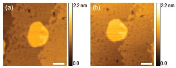
Fig. 3. Topography image of a3-4 layer MoS2 (a) initially and (b) after
5 successive scans at 0.1 V set point using a PPP-NCSTPt probe with
spring constant of ~7 N/m. Scale bar is 50 nm.
C-AFM + LFM for Grain Boundary Analysis
When imaging with a low spring constant probe, such as PPP-CONTSCPt with nominal spring constant of 0.2N/m, we can acquire frictional data simultaneously with C-AFM, allowing for correlation between topographic, electrical, and material properties. Figure 3 shows the height, friction, and current images from a 1-2 layer MoS2 sample. The 1st layer and 2nd layer regions are labeled as 1Ly and 2Ly, respectively, in figure 3(a). The friction at grain boundaries is higher than the pristine regions, so that they show up as dark lines in the friction. By comparing the current and friction, we can see that the dark lines in the friction image match the dark lines in the current. However, the current image shows additional features due to the influence of the substrate on the local conductivity of the 2D film.
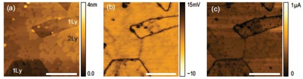
Fig. 4. (a) Topography, (b) Friction, and (c) current acquired
simultaneously on an 1-2 layer as-grown MoS2 / sapphire sample.
The layer thickness of each region is indicated in (a). Scale bar is 200 nm.
Scanning Tunneling Microscopy on MoS2
With the Park NX-Hivac, we were able to also acquire high quality STM images without the need for complicated UHV systems and special sample prep/handling. Figure 4 shows a 500 nm scan of the multi-layer MoS2 sample imaged in constant current mode, with Iset=0.5 nA and Vbias = 1 V. Since STM gives a convolution of topography with electronic structure, we see both islands and grain boundaries in the height image.
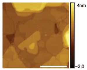
Fig. 5. STM image of multilayer MoS2 / sapphire.Cut Pt-Ir wire in
constant current mode. Iset = 0.5 nA, Vbias = 1 V. Scale bar is 200 nm.
Conclusion
In this study, molybdenum disulfide (MoS2), one of the highly interesting 2D materials of transition metal dichalcogenides (TMDs) family, was investigated on morphological and electrical aspects using Park NX-Hivac AFM (Park Systems). The differences between single and multi-layer was observed on AFM topography images. Furthermore, the details of 3D pyramid-like structures due to layer-by-layer growth mechanism was determined at multi-layer image.
Using conducting SPM (C-AFM and STM), electrical properties of MoS2 were studied both in ambient and high vacuum (HV) condition. Despitethe presence of oxide layer, clear, homogeneous and higher current signal was measured while in HV condition. Lastly, topographical, electrical, and mechanical information were obtained for grain boundary analysis using combination of C-AFM and LFM. This approach allowed the finding of more specific and detailed structures on grain boundary.
2D layered material is widely used for various research field both industry and academy. The characterization and exploration of electrical and mechanical properties of 2D material are one of the most critical pointsin materials research field. The atomic force microscope, a versatile imaging and measurement tool, allows us to evaluate 2D materialsin multidirectional viewpoints using various imaging modes. This study underlines the improving strategy of material analysis. Moreover, these results emphasize the importance of multidirectional and multichannel analysis on 2D materials, including the transition metal dichalcogenides that are of high interest by the semiconductor industry.
References
1. K. S. Novoselov, A. Geim, S. V. Morozov, D. Jiang, Y. Zhang, S. V. Dubonos, I. V. Grigorieva, &A. A. Firsov. Electric field effect in atomically thin carbon films. Science306, 666–669 (2004).
2. A. K. Geim & I. V. Grigorieva. Van der Waals heterostructures. Nature499, 419–425 (2013).
3. K. F. Mak, C. Lee, J. Hone, J. Shan, & T. F. Heinz. Atomically Thin MoS2: A New Direct-Gap Semiconductor. Phys Rev Lett105,136805 (2010).
4. H. Liu, A. T. Neal, Z. Zhu, Z. Luo,X. Xu, D. Tománek,&P. D. Ye. Phosphorene: an unexplored 2D semiconductor with a high hole mobility. ACS Nano8, 4033–4041 (2014).
5. J. Zhao, H. Liu, Z. Yu, R. Quhe, S. Zhou, Y. Wang, C. C. Liu, H. Zhong, N. Han, J. Lu, Y. Yao,&K. Wu. Rise of silicene: A competitive 2D material. Prog Mater Sci83, 24–151 (2016).
6. C. R. Dean, A. F. Young, I. Meric, C. Lee, L. Wang, S. Sorgenfrei, K. Watanabe, T. Taniguchi, P. Kim, K. L. Shepard, & J. Hone.Boron nitride substrates for high-quality graphene electronics. Nat Nanotechnol5, 722–726 (2010).
7. X. Xu, W. Yao, D. Xiao, &T. F. Heinz. Spin and pseudospins in layered transition metal dichalcogenides. Nat. Phys.10, 343–350 (2014).
8. G. Fiori, F. Bonaccorso, G. Iannaccone, T. Palacios, D. Neumaier, A. Seabaugh, S. K. Banerjee,& L. Colombo. Electronics based on two-dimensional materials. Nat Nanotechnol9, 768–779 (2014).
9. X. Xi, L. Zhao,Z. Wang, H. Berger, L. Forró, J. Shan,& K. F. Mak. Strongly enhanced charge-density-wave order in monolayer NbSe2. Nat. Nanotechnol.10, 765–769 (2015).
10. S. Manzeli, D. Ovchinnikov, D. Pasquier, O. V. Yazyev, &A. Kis. 2D transition metal dichalcogenides. Nat. Rev. Mater.2, 17033 (2017).
11. W. Choi, N. Choudhary, G. H. Han, J. Park, D. Akinwande,&Y. H. Lee. Recent development of two-dimensional transition metal dichalcogenides and their applications. Mater. Today20, 116–130 (2017).
12. D. Chiappe, J. Ludwig, A. Leonhardt, S. El Kazzi, A. Nalin Mehta, T. Nuytten, U. Celano, S. Sutar, G. Pourtois, M. Caymax, K. Paredis, W. Vandervorst, D. Lin, S. Degendt, K. Barla, C. Huyghebaert, I. Asselberghs, and I. Radu, Layer-controlled epitaxy of 2D semiconductors: bridging nanoscale phenomena to wafer-scale uniformity. Accepted Nanotechnology (2018).
13. E. R. Dobrovinskaya, L. A.Lytvynov,& V. Pishchik. Sapphire: material, manufacturing, applications. Springer Science & Business Media, 2009.
14. B. Radisavljevic, A. Radenovic, J. Brivio, V. Giacometti, & A. Kis. Single-layer MoS2 transistors. Nat Nanotechnol6, 147–150 (2011).
15. A. Leonhardt, D. Chiappe, I. Asselberghs, C. Huyghebaert,&I. Radu. Improving MOCVD MoS2 Electrical Performance: Impact of Minimized Water and Air Exposure Conditions. IEEE Electron Device Lett38(11) 1606-1609 (2017).