


Dr. Gwo-Ching Wang, Dept. of Physics, Applied Physics & Astronomy, Rensselaer Polytechnic Institute
Dr. Gwo-Ching Wang, received her PhD degree from University of Wisconsin, worked at NBS Washington, DC and Oak Ridge National Laboratory before joining Rensselaer. She is the Rensselaer Travel stead Institute Chair. She served as the head of the Physics Department at Rensselaer Polytechnic Institute (2000-2010). Her thin film and nanostructure physics lab is equipped with Park Systems AFM, high-resolution low energy electron diffraction (HR-LEED), reflection high energy electron diffraction (RHEED) and surface magneto optical Kerr effect (SMOKE) to study surface morphology, structure and magnetic properties of materials. The group members also developed RHEED reciprocal space mapping to study graphene and TMDC monolayer as well as RHEED pole figure analysis to study texture of thin films and nanostructures.
In the past decade there has been a worldwide research interest in two-dimensional materials such as graphene (one layer of graphite), transition metal dichalcogenides (TMDCs), and 2D oxides(mica, layered Cu oxides, etc.)1. A bulk TMDC consists of astack of MX2 monolayers. Each MX2 consists of X− M−X where M is a transition metal atom (Mo, W, V, Nb, etc.) sandwiched between two X chalcogen atoms (S, Se, or Te). See Fig. 1(a). The out-of-plane interaction between MX2 is weak van der Waals (vdW) interaction and the in-plane interaction is strong chemical interaction.
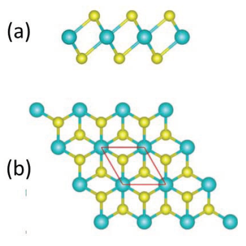
Fig. 1 (a) Side view and (b) top view of a VS2 monolayer in octahedral 1T phase. The V and S atoms are in blue and gold, respectively. The red parallelogram is a two dimensional unit cell. [From Ref. 8] Figure 1(b)is a top view of one monolayer of vanadium disulfide (VS2).
Among over 40 low-dimensional TMDCs, most are semiconducting dichalcogenides. Low-dimensional vanadium disulfide (VS2) is one of the metallicdichalcogenides.On the theoretical side, first principles spin polarized density function theory (DFT) calculations predict that a large magnetic moment exists in a free standing VS2 monolayer form due to the quantum size eff ect2-9. DFT calculations also predict the existence of magnetic moments for a few monolayer thick VS26. These DFT predictions extended the potential of electrons in the controls and manipulations of electronic and magnetic properties of TMDCs that may enable electronic/spintronics applications.
The vdW TMDC crystals have been shown experimentally to possess many fascinating mechanical, optical and electronic properties. However, there have been fewer studies on the magnetic property of vdW TMDC crystals, because most TMDC crystals are nonmagnetic in the bulk forms. Practical methods such as defect engineering 10 have been designed to extrinsically induce magnetism within these vdW TMDC materials with the hope to observe magnetism. The challenges in the synthesis of low-dimensional TMDCs are the control of thickness, size and stoichiometry. Take VS2 as an example. Hydrothermal 11-14,liquid exfoliation 15, and chemical vapor deposition (CVD) 16, 17 methods have produced VS2 nanosheets, nanoplates, and nanoflowers. These nanostructures have been applied in battery anodes17, 18, supercapacitors13, moisture sensor19, and electrocatalytic hydrogen evolution reaction (generating hydrogen by splitting water)14, 16. Despite the possibility that defects or impurities or substrates from these synthesis methods may contribute or influence the intrinsic magnetic property of nanostructure VS2, there are signs of magnetic signals from these nanostructures measured by vibrating sample magnetometer(VSM) orsuperconducting quantum interference device SQUID 11, 12, 20.One exciting work of monolayer (ML) and nanoflowers. These nanostructures have been applied in battery anodes17, 18, supercapacitors13, moisture sensor19, and electrocatalytic hydrogen evolution reaction (generating hydrogen by splitting water)14, 16. Despite the possibility that defects or impurities or substrates from these synthesis methods may contribute or influence the intrinsic magnetic property of nanostructure VS2, there are signs of magnetic signals from these nanostructures measured by vibrating sample magnetometer(VSM) or super conducting quantum interference device SQUID 11, 12, 20. One exciting work of monolayer (ML) and few ML VSe2 (Se is in the same chalcogens column) grown by molecular beam epitaxy in ultra high vacuum was reported to show strong room temperature ferromagnetism measured by VSM and surface magneto optical Kerr effect (SMOKE) ex situ using a Se capping layer 21.
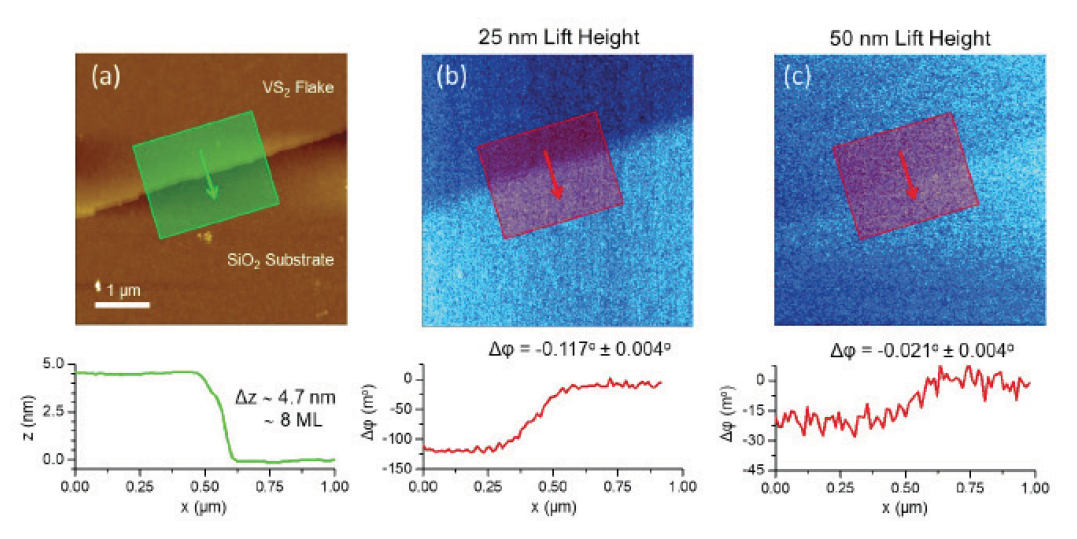
Fig. 3 An ultrathin VS2 flake on the SiO2 substrate. (a) AFM topography scan revealing the flake thickness to be ~ 4.7 nm thick, corresponding to eight S-V-S layers. MFM phase map of the area shown in (a), collected at a lift height (L) of (b) 25 nm and (c) 50 nm. Scale bars in (a) is 1 μm.
We have used CVD targeting at synthesizing monolayer and ultrathin VS2 films and search for room temperature ferromagnetic ordering in the films. The precursor used was VCl3 and sulfur vapor came from heated S powders. The growth parameters were systematically tested by varying the S powder amount, VCl3 precursor amount, carrier gas type, carrier gas flow rate, heating zone temperatures and the growth duration. Under the optimum CVD growth condition various sizes and thicknesses of flakes were observed on SiO2 substrate. Flake sizes ranged from a few microns to about 100 microns. The flake thicknesses ranged from sub-tens nm to 200 nm. Fig. 2(a) is an example of many large and thick flakes on SiO2. Monolayer and bilayer were also observed but rare. The surface of the large flake is smooth as seen in the 50 μm × 50 μm AFM image in Fig. 2(b). Figure 2(c) shows a height scan along the white line on the surface of the flake in Fig. 2(b). The height variation is within one or two nm over 50 μm. On the surface there are 3 nm spikes occasionally observed.
The Energy Dispersive Spectroscopy of these flakes shows approximately 1 to 2 stoichiometry ratio of V to S with slightly V rich.
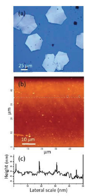
Fig. 2 (a) Optical image of VS2 flakes grown on SiO2 substrate by chemical vapor deposition. (b) AFM image of an ultrathin flake larger than 50 μm. (c) Height scan along the surface of the flake indicated as a white dashed line in (b).
To study the magnetic property of ultrathin VS2 flakes on SiO2 substrate, we use AFM first to identify the flake and then measure the magnetic phase contrast using magnetic force microscopy(MFM) at room temperature. A Park Systems NX20 scanning probe microscope with a Park MFMR cantilever (k ~ 2.8 Nm-1, selected frequency ~ 75 kHz, CoCr coated with nominal coercivity ~ 400 Oe) was used for MFM measurements.
Both the sample and tip were magnetized by a ~ 500 Oe permanent magnet prior to image collection. The MFM22 data collection began with a traditional non-contact AFM scan to map the sample’s topography by measuring the attractive van der Waals forces between the sample and the probe tip23. After acquiring the topography data, the tip was lifted to a pre-set distance (typically 20 – 50 nm) beyond the influence of the vdW forces. It then followed the collected topography line scan to maintain a constant sample probe distance and detected the magnetic interactions via a shift in the cantilever’s vibrational phase.
Figure 3 shows an AFM topography and MFM phase maps of a VS2 flake on SiO2. The optical image (not shown here) indicates an ultrathin flake with a diameter of about 20 μm that is visible due to an optical interference with the 300 nm SiO2/Si substrate. Figure 3(a) shows a AFM topography map of the edge of a flake which gives the flake’s thickness to be ~ 4.7 nm, corresponding to eight S-V-S layers. An MFM phase map collected at a lift height of 25 nm is shown in Fig. 3(b). The negative phase shift of the sample relative to the SiO2 substrate, which is weakly diamagnetic (essentially non-magnetic), indicates an attraction between the VS2 flake and the MFM cantilever. This phase contrast was not observed when the sample and tip were not magnetized. Furthermore, because one phase contrast was measured across the whole of each flake, one can infer that each flake is composed of just one magnetic domain. This measurable magnetic interaction implies the existence of a remanent magnetization at room temperature in the sample, a property of ferromagnetic materials.
To demonstrate the dependence of MFM phase contrast on the sample-tip distance, data were collected at the lift heights (L) of 50 nm shown in Fig. 3(c). Qualitatively, the interfacial phase contrast decreases with an increase in L. Averaging over approximately 50 line scans in the framed box across the flake/substrate interface ensures the data’s reliability and provides optimal signal-to-noise ratio. The decay of the MFM phase shift with an increase in lift height likewise indicates a decrease in the attractive force between the tip and sample, consistent with what one would expect for a magnetic interaction24-26. The observation of the MFM phase signal reveals the existence of ferromagnetism in the ultrathin VS2 film consistent with density functional theory calculations6. This negative MFM phase shift was reproducibly measured for several flakes ranging in thickness from 5 nm to 20 nm with consistent results. In fact, slightly stronger phase signal ( indicating stronger magnetization) was measured as thickness decreased, consistent with the theoretical predictions6.
Through the use of magnetic force microscopy, room temperature ferromagnetism has been detected in ultrathin VS2 crystalline flakes grown by CVD. This property does not exist in the bulk VS2 material, but arises due to quantum confinement effects resulting from a reduced dimensionality. This is of significance to both fundamental physics, of which the study of ultrathin layered materials (and specifically transition metal dichalcogenides such as VS2) is a field attracting much attention. We learned that CVD growth of low-dimensional VS2 materials, including monolayer (ML) thickness, remains challenging. A better controllable method to grow monolayer VS2 is molecular beam epitaxy in ultra high vacuum 21, 27. Different monolayer of magnetic TMDC can be stacked to form artificial heterostructures that have the potential application to emerging research areas including future high density storage and spintronics.
Acknowledgement
The CVD growth of ultrathin VS2 flakes was performed by Z. Li and A.J. Littlejohn. The AFM and MFM images were collected by A.J. Littlejohn with the assistance from Dr. Wenqing Shi at Park Systems. Graduate student Yu Xiang (see photo) uses AFM extensively for morphological study of graphene and TMDC materials. He gave a talk entitled “2D Materials in Real and Reciprocal Spaces: Complimentary AFM and RHEED Studies”at the NanoScientific Symposium on SPM in Sept. 2018.This work is supported by the New York State’s Empire State Development’s Division of Science, Technology and Innovation (NYSTAR) through Focus Center Contract C150117. Graduate student Yu Xiang uses Park Systems’ AFM in the Rensselaer lab. Graduates from the ulta thin film physics and nanoscience lab are working at US industries or universities making contributions to the advancement of science and technology. Examples of research areas are non-equilibrium growth and etching of metal and semiconductor films, magnetism of ultrathin magnetic films and dots, transport properties of metallic and magnetic films and nanotubes, fabrication and growth mechanism of sculptured films. The lab has been equipped with state of the art commercial and homemade techniques for fabrication and characterization of novel nanostructures. Examples of real space and diffraction techniques are scanning tunneling microscopy (STM), atomic force microscopy (AFM), nanolithography, high resolution low energy electron diffraction (HRLEED), energy filtered reflection high energy electron diffraction (EFRHEED), angle resolved light scattering (ARLS), Auger electron spectroscopy (AES), x-ray photoelectron spectroscopy (XPS), four point probe, magneto optic Kerr effect (MOKE), magnetoresistance, and ferromagnetic resonance. Examples of growth/etching techniques include thermal evaporation, chemical vapor deposition, atomic layer deposition, oblique angle incidence deposition, and ion sputtering. Physical properties of these nanostructures including
magnetic, mechanical, electrical, transport, and structural are characterized by these surface sensitive techniques.
References
1. Geim, A. K.; Grigorieva, I. V., Van der Waals heterostructures. Nature 2013, 499, 419-425.
2. Ataca, C.; Şahin, H.; Ciraci, S., Stable, Single-Layer MX2 Transition-Metal Oxides and Dichalcogenides in a Honeycomb- Like Structure. The Journal of Physical Chemistry C 2012, 116, 8983-8999.
3. Ma, Y.; Dai, Y.; Guo, M.; Niu, C.; Zhu, Y.; Huang, B., Evidence of the Existence of Magnetism in Pristine VX2 Monolayers (X = S, Se) and Their Strain-Induced Tunable Magnetic Properties. ACS Nano 2012, 6, 1695-1701.
4. Zhou, Y.; Yang, C.; Xiang, X.; Zu, X., Remarkable magnetism and ferromagnetic coupling in semi-sulfuretted transition-metal dichalcogenides. Physical Chemistry Chemical Physics 2013, 15, 14202-14209.
5. Zhang, Y.; Wu, X., Vanadium sulfide nanoribbons: Electronic and magnetic properties. Physics Letters A 2013, 377, 3154- 3157.
6. Zhang, H.; Liu, L.-M.; Lau, W.-M., Dimension-dependent phase transition and magnetic properties of VS2. Journal of Materials Chemistry A 2013, 1, 10821-10828.
7. Kan, M.; Wang, B.; Lee, Y. H.; Sun, Q., A density functional theory study of the tunable structure, magnetism and metal– insulator phase transition in VS2 monolayers induced by in-plane biaxial strain. Nano Res. 2015, 8, 1348-1356.
8. Wasey, A. H. M. A.; Chakrabarty, S.; Das, G. P., Quantum size effects in layered VX2 (X=S, Se) materials: Manifestation of metal to semimetal or semiconductor transition. J Appl Phys 2015, 117, 064313.
9. Zhuang, H. L.; Hennig, R. G., Stability and magnetism of strongly correlated single-layer VS2. Physical Review B 2016, 93, 054429.
10. Wang, Y.; Tseng, L.-T.; Murmu, P. P.; Baoc, N.; Kennedy, J.; Ionesc, M.; Ding, J.; Suzuki, K.; Li, S.; Yi, J., Defects engineering induced room temperature ferromagnetism in transition metal doped MoS2. Materials and Design 2017, 121, 77-84.
11. Gao, D.; Xue, Q.; Mao, X.; Wang, W.; Xu, Q.; Xue, D., Ferromagnetism in ultrathin VS2 nanosheets. Journal of Materials Chemistry C 2013, 1, 5909-5916.
12. Zhong, M.; Li, Y.; Xia, Q.; Meng, X.; Wu, F.; Li, J., Ferromagnetism in VS2 nanostructures: Nanoflowers versus ultrathin nanosheets. Materials Letters 2014, 124, 282-285.
13. Feng, J.; Sun, X.; Wu, C.; Peng, L.; Lin, C.; Hu, S.; Yang, J.; Xie, Y., Metallic Few-Layered VS2 Ultrathin Nanosheets: High Two-Dimensional Conductivity for In-Plane Supercapacitors. Journal of the American Chemical Society 2011, 133, 17832- 17838.
14. Liang, H.; Shi, H.; Zhang, D.; Ming, F.; Wang, R.; Zhuo, J.; Wang, Z., Solution Growth of Vertical VS2 Nanoplate Arrays for Electrocatalytic Hydrogen Evolution. Chemistry of Materials 2016, 28, 5587-5591.
15. Coleman, J. N.; Lotya, M.; O’Neill, A.; Bergin, S. D.; King, P. J.; Khan, U.; Young, K.; Gaucher, A.; De, S.; Smith, R. J.; Shvets, I. V.; Arora, S. K.; Stanton, G.; Kim, H.-Y.; Lee, K.; Kim, G. T.; Duesberg, G. S.; Hallam, T.; Boland, J. J.; Wang, J. J.; Donegan, J. F.; Grunlan, J. C.; Moriarty, G.; Shmeliov, A.; Nicholls, R. J.; Perkins, J. M.; Grieveson, E. M.; Theuwissen, K.; McComb, D. W.; Nellist, P. D.; Nicolosi, V., Two-Dimensional Nanosheets Produced by Liquid Exfoliation of Layered Materials. Science 2011, 331, 568-571.
16. Yuan, J.; Wu, J.; Hardy, W. J.; Loya, P.; Lou, M.; Yang, Y.; Najmaei, S.; Jiang, M.; Qin, F.; Keyshar, K.; Ji, H.; Gao, W.; Bao,J.; Kono, J.; Natelson, D.; Ajayan, P. M.; Lou, J., Facile Synthesis of Single Crystal Vanadium Disulfide Nanosheets by Chemical Vapor Deposition for Efficient Hydrogen Evolution Reaction. Advanced Materials 2015, 27, 5605-5609.
17. Ji, Q.; Li, C.; Wang, J.; Niu, J.; Gong, Y.; Zhang, Z.; Fang, Q.; Zhang, Y.; Shi, J.; Liao, L.; Wu, X.; Gu, L.; Liu, Z.; Zhang, Y., Metallic Vanadium Disulfide Nanosheets as a Platform Material for Multifunctional Electrode Applications. Nano Letters 2017, 17, 4908-4916.
18. Liu, J.-Z.; Guo, P.-F., VS2 Nanosheets: A Potential Anode Material for Li-ion Batteries. Journal of Inorganic Materials 2015, 30, 1339-1344
19. Feng, J.; Peng, L.; Wu, C.; Sun, X.; Hu, S.; Lin, C.; Dai, J.; Yang, J.; Xie, Y., Giant Moisture Responsiveness of VS2 Ultrathin Nanosheets for Novel Touchless Positioning Interface. Advanced Materials 2012, 24, 1969-1974.