


High Resolution Phase Imaging of Polymer Thin Film Coated on Gold (Au)
John Paul Pineda, Charles Kim, Byong Kim, and Keibock Lee
Park Systems Inc., Santa Clara, CA USA
INTRODUCTION
Functional polymer thin filmshave numerous technological applications ranging from optoelectronics to sensors. Theirtunable properties, flexibility, and low-cost preparation make them attractive to the industry. [1]The properties of polymer thin films are heavily affected by the distribution, shapes, and monomer composition of individual macromolecules. For this reason, designing polymer properties requires a characterization technique that canimage material contrasts with high spatial resolutions to visualize the polymer morphologyon the nanoscale and measuremacromolecule sizes accurately.[2] Scanning Electron Microscopy (SEM) and Energy-filtered transmission electron microscopy (EFTEM) are common methods to characterize polymer thin films. However, SEM has a low spatial resolution when imaging nanostructured organic samples containing light elements only, while EFTEM has high level of knock-on damage due to high accelerating voltages applied during operation. [3, 4]An effective tool to overcome these problems is Atomic Force Microscopy (AFM). AFM is a nondestructive technique that provideshigh-resolution images required for nanoscale characterization. Moreover, this tool can be operated in different measurement modes that image material properties in addition to topological information.Among these, Phase Imaging is a powerful AFM mode used by scientists and engineers to study compositional heterogeneities in polymer materials.This mode provides complementary information to the topography image by revealinglocalvariations of surface properties and compositionsinthe investigated materials.
In this study, a Park NX20 was used to characterize polymer thin filmscoated on Gold(Au) using Tapping Mode AFM. A high-resolution phase image acquired simultaneously with the topography imagerevealed that surface changes occurred after heating the sample and applying DC tip bias. The conformation and phase separation of the polymer domains were measured and evaluated.
EXPERIMENTAL
A polymer thin film coated on Au on a silicon wafer was heated up to 230ıCusing a Park Systems temperature control stage.Additionally a 1V DC voltage was applied between the AFM tip and the sample surface.With aPark NX20, both topography and phase image were obtained simultaneously by using Tapping Mode AFM under ambient conditions. Imageswere acquiredbefore and after the sample had undergonethe heating process and tip bias application. A conductive MikromaschNSC36A Ti-Pt cantilever (nominal spring constant k = 1 N/m and resonant frequency f = 90 kHz) was used in the experiment.
RESULTS AND DISCUSSION
In Tapping Mode, the tip oscillates near its resonance frequency, which allows the tip to periodically touch the sample surface at the lower turning point of the oscillation.Topography images are obtained by measuring the changes in the vibrational amplitude of the cantilever induced by the attractive Van-der-Waals force as the cantilever is mechanically oscillated near its resonant frequency during the scan. The measured changes are compensated by the AFM’s feedback loop, which maintains the cantilever’s constant amplitude and distance by controlling the Z scanner movement. [5]The phase image is acquired simultaneously by monitoring the phase lag between the signal that drives the cantilever oscillation and its output signal, as shown in Figure 1.
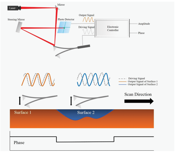
Figure 1. Schematic Illustration of Phase Imaging [6].
Table 1 shows the topography and phase images of a polymer thin filmbefore and afterheating and bias application.The topography image acquired before the treatmentreveals asmooth sample surface, while the phase image showsthat the surface was composed of lamellar polymer fibrilsdistributed homogeneously over the surface.On the other hand, the topography acquired after the heat and bias treatment revealsthat two circular protrusions (inner and outer protrusions) formed in the center of the scanned surface. The inner circular protrusionhas a height of around 53 nm and a diameter ranging from 1.4 to 2.0μm. The outside circular protrusionhas a lower height of around 30 nm anda diameter ranging from 2.0 to 4.0μm. Thesurrounding area isrelatively flat with a mean square surface roughness of 0.8 nm.By comparing topography and phase image, it could be observed that the orientation of the lamellar fibrils in the inner and outer circular protrusions is re-arranged and the fibrils are aligned differentlyin both protrusions as well as the flat surface.
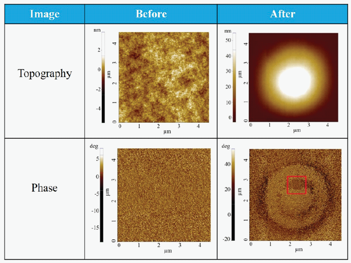
Table1:Topography and Phase image before and after heating the sample at 230ıC and applying 1V DC voltage between the sample and the tip.
Figure 2a and 2bare the enlarged view and corresponding 3D representation of the area highlighted in red in the phase image of Table 1.Both images clearly show distinct differences in the fibril alignment.As such the upper and lower part of Figure 2a captured periodic fibrils align in-plane, while the dotted area in the center of the Figure corresponds to domains with fibrils that re-arranged inthe vertical direction during the heat and bias treatment. Figure 2c is the corresponding line profile generated using Park XEI image analysis software to evaluate the sizes of the lamellar fibrilsas well as phase separation. The measured width of the lamellar fibrilswas approximately 26 nm, while separation between each fibrils was approximately 22 nm.
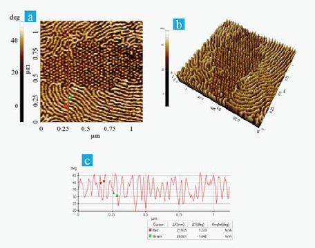
Figure 2. (a) Enlarged view of the phase image in table 1 (after heat and bias treatment),
(b) 3D view of Figure 2a, (c) Corresponding line profileof Figure 2a.
SUMMARY
This study demonstrates the suitability of phase imaging for the characterization of polymer thin films. The high-resolution phase images obtained in the experiment reveals significant surface changes of the polymer thin films after they underwent heating and bias application. It is observed that during the heat and bias application, some polymer fibrils re-aligned to a vertical orientation and others remained in-plane. Additionally, the in-plane fibrils formed domains of varying orientations. Thus, phase imaging can provide unique insights of how temperature and DC voltage affect the fibril arrangement and orientation of polymer thin films, as required to design customized properties. Since phase imaging operates in AFM tapping mode, this technique allows safe acquisition of high-resolution images without the continuous tip-sample contact. In sum, phase imaging is a promising tool in applications that require high-resolution imaging of material contrasts on the nanoscale.
REFERENCES
1. S. Satish, et al., Preparation and characterization of nanoscale PMMA thin films Indian Journal of Pure & Applied Physics. Vol. 52, January 2014, pp. 64-67.
2. V. Korolkov, et al., Ultra-high resolution imaging of thin films and single strands of polythiophene using atomic force microscopy. Nature Communications volume 10, Article number: 1537 (2019)
3. J. Brostin, Compositional Imaging of Polymers Using a Field Emission Scanning Electron Microscope with a Microchannel Plate Backscattered Electron Detector. SCANNING Vol. 17, 327–329 (1995). Received March 13, 1995 and Accepted with revision May 22, 1995.
4. R. Masters, et al., Sub-nanometre resolution imaging of polymer–fullerene photovoltaic blends using energy-filtered scanning electron microscopy. Nature Communications volume 6, Article number: 6928 (2015)
5. https://www.parksystems.com/images/spmmodes/standard/3_Phase-Imaging-and-Phase- Detection-Microscopy-(PDM).pdf
6. J. Gunther, Introduction to Atomic Force Microscopy, March 10, 1998, ACS Group and MENs, Beckman Institute. https://www.slideshare.net/joserabelo/atomic-force-microscopy-37962055