

Photovoltaic effect in ferroelectric materials
(by using Piezoresponse Force Microscopy PFM)
Wednesday, 17 June 2020
- 10:00 am – 11:30 am
(GMT)
London, Dublin - 11:00 am – 12:30 pm
(CEST)
Berlin, Paris, Rome - 17:00 pm - 18.30 pm
[GMT+8]
Beijing, Singapore - 18:00 pm – 19:30 pm
[UTC+9]
Seoul, Tokyo
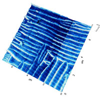
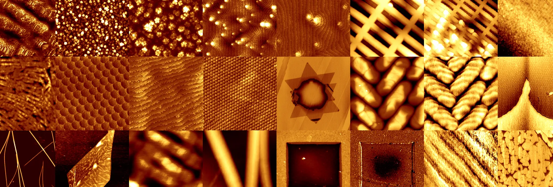
Photo-current signal acquired with Conductive-AFM from domain walls in BiFeO3
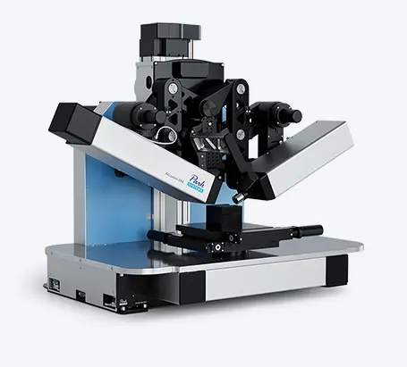
Observation of photovoltaic effect in ferroelectric thin films has been of great relevance for the field of multiferroics and photovoltaics. While this adds yet another functionality to multiferroics, generation of photocurrent in the absence any junction provides an exciting platform for studying a new charge separation mechanism. In this regard, scanning probe microscope can be considered as one of the most powerful techniques for investigating material properties on a nanoscale. The properties that can be measured are determined by the type of the probe. In the case of an electrically conductive probe, ac and dc signals can be used to analyze the photo-conductive, piezoelectric and ferroelectric character of the material.
In this talk, thin films of epitaxially grown BiFeO3 and Pb(Zr,Ti)O3 will be used to demonstrate the photoelectrical response from ferroelectric materials. Piezoresponse force microscope was utilized to confirm the ferroelectric character of the samples and analyze the domain arrangements. Macro-scale measurements were conducted to extract the photoelectrical response. A clear bulk-driven photovoltaic effect was visible in BiFeO3 films which was found to be in a rather intricate correlation with in-plane polarization. In the case of PZT films, apart from a photovoltaic effect, light induced a surprising enhancement in the conductivity of the samples which was found to decay over time, i.e. persistent photoconductivity. The results therefore showcase manifestation of two characteristics, photovoltaic effect and persistent photoconductivity, that are conventionally associated with semiconductors, in ferroelectric materials.

Presenter:
Dr. Akash Bhatnagar,
The Centre for Innovation Competence SiLi-nano®
Martin Luther University of Halle-Wittenberg, Germany
akash.bhatnagar@physik.uni-halle.de
Akash is a Group Leader at Zentrum für Innovationskompetenz SiLi-nano in Halle. The primary focus of his group is synthesis and characterization of ferroelectric/multiferroic materials for functional applications. His expertise includes thin film growth, surface probe microscopies and transport measurements. Prior to this position, Akash received his Doctorate at Max Planck Institute of Microstructure Physics while working in the group of Prof Dietrich Hesse, and subsequently worked as a Research Fellow at University of Warwick, UK in the group of Prof. Marin Alexe.