


How it works
What is Pinpoint™?
PinPoint is a proprietary operation mode of Park Systems AFMs that provides accurate and quantitative nanomechanical images via fast force spectroscopy mapping. Besides the acquisition of nanomechanical properties, including adhesion force and elastic modulus, the controlled contact force and time in PinPoint allows more accurate and less invasive electrical and electromechanical imaging. In Park AFMs, PinPoint combines several traditional modes of second generation AFMs into one potent and customizable package.
How does Pinpoint work?
In PinPoint mode, the cantilever approaches and retracts at each pixel
of the entire scan area to simultaneously acquire 3D topography and nanomechanical information of
the sample surface (for example 256x256 pixel = 65536 measurement
points).
At each pixel, the XY scanner stops and high-speed force-distance curves are taken
with well-defined control of contact force and contact time between the tip and the sample.
What does PinPoint mode offer?
PinPoint mode has the capability to simultaneously collect topography,
stiffness, elastic modulus, and adhesion forces in real-time. By moving the tip in an
approach-retract technique with forces down to a few nano Newton, PinPoint ensures
a frictionless operation that eliminates the shear force and therefore preserves tip and sample
condition.
Furthermore, PinPoint can be combined with electrical and electromechanical
measurement modes, allowing a non-invasive
characterization of soft samples, that are sensitive to shear forces.
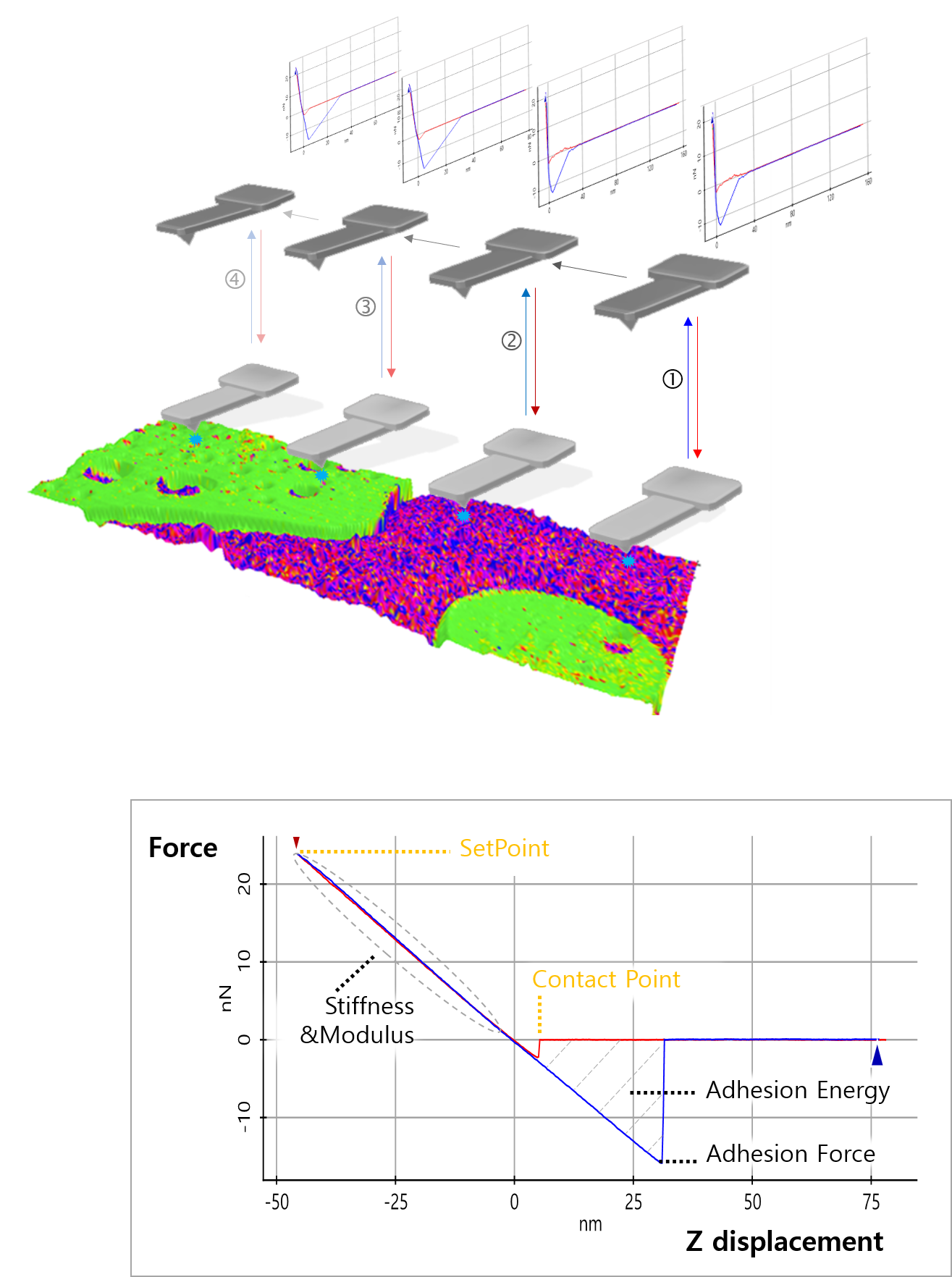
Working principle of PinPoint™ nanomechanical mode by Park
Systems.
The probe is moved from point 1 to 5, and at each point force-distance curves are taken to calculate the nanomechanics each point.
PinPoint mode for investigating electrical and electromechanical properties
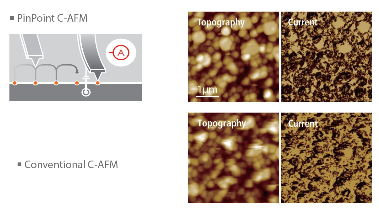
PinPoint cAFM
PinPoint PFM for enhanced electrical investigation at nanoscale
PinPoint cAFM performs conductive measurements with higher accuracy for both topography and
current measurements compared to traditional cAFM, due to:
- a reduction of shear force that preserves the tip quality and lifetime and thereby increases the repeatability,
- higher spatial resolution as result of lower tip wear,
- controlled contact force and time for highly accurate current detection,
- defined contact force that preserves the sample integrity, particularly on soft, polymeric surfaces,
- simultaneous acquisition of conductive, topographical and nanomechanical sample properties.
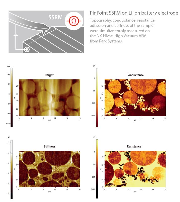
PinPoint SSRM
PinPoint SSRM for optimal results in semiconductor applications
In comparison to traditional SSRM operation, PinPoint SSRM improves the data acquisition
by:
- reducing shear forces for longer tip lifetime and reduced sample damage
- offering a more accurate detection of the electrical signals due to controlled contact force and time
- simultaneous acquisition of current, conductance, resistance, topography and nanomechanical properties.
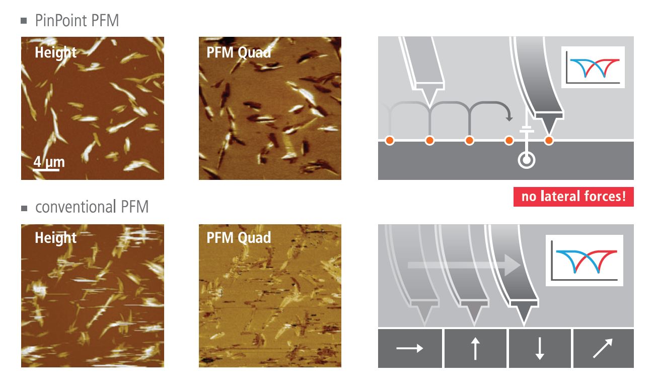
PinPoint PFM
PinPoint PFM for enhanced electrical investigation at nanoscale
In comparison to conventional contact PFM, PinPoint PFM non-invasively acquires topography
and piezoelectric data on soft, polymeric samples, as PinPoint PFM provides:
- controlled contact force and time for repeatable and accurate piezoresponse measurements,
- high spatial resolution due to reduced tip wear,
- non-invasive imaging particularly for soft samples by reduction of shear forces,
- simultaneous acquisition of piezoresponse, topography and nanomechanical properties.
Application Examples
Failure Analysis and Defect Recognition

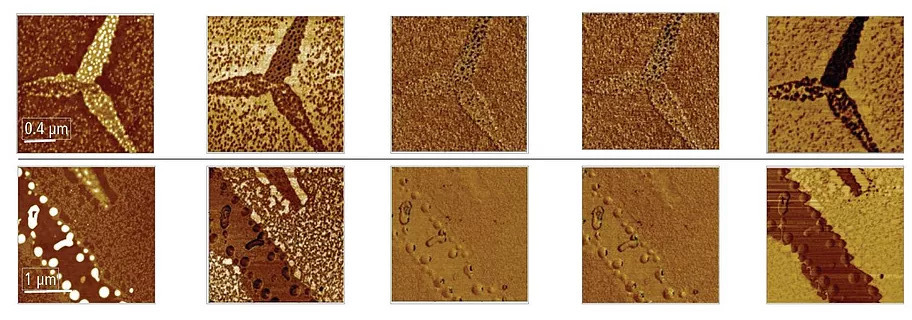
PinPoint cAFM allows the characterization of electrical designs of semiconductor devices like SRAMs with the high accuracy, precision and repeatability required for failure analysis, due to:
- the controllable data acquisition time allowing a very high signal-to-noise ratio,
- frictionless conductivity scanning,
- reproducible data from repeated measurements,
- cost savings from longer lasting AFM probe tips.
Failure analysis of semiconductor device via PinPoint cAFM
- A leakage current was observed on a component of the faulty device (leaking component marked by yellow arrow).
- Leakage current originates from a contact of the n-doped area below the faulty device component.
Cell biology and other life science applications
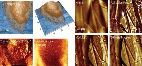
PinPoint mode offers accurate nanomechanical imaging of biological samples via:
- mapping of nanomechanical properties including adhesion force, elastic modulus, stiffness and deformation plus topography with nanometer resolution,
- fast, quantitative imaging of elasticity distribution with a correlated topography map, which reveals the position and orientation of sample,
- simultaneous acquisition of topography and FD data avoids positional errors as well as sample damage such as scratches or streak marks, frequently observed in traditional AFM imaging of cells or biological samples in liquid.
Cell mechniacal properties measured via PinPoint nanomechanical mode
Polymer Science
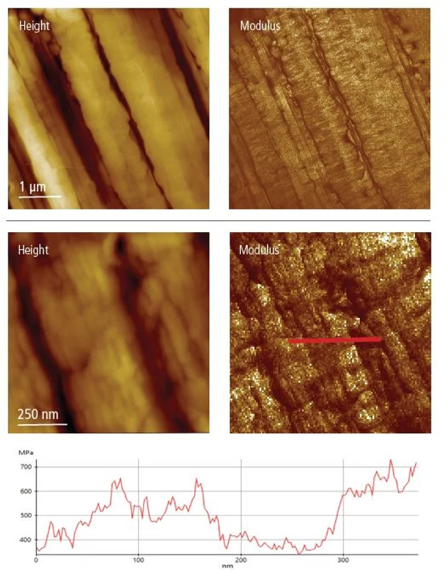
PinPoint Nanomechanical imaging on commercial Teflon polymer
High resolution nanomechanical map of DMT Modulus on a sample of commercial Teflon tape. The average modulus is ~400 MPa. On crystalline areas it reaches 500-600 MPa.
The graph shows a cross-sectional profile from modulus image, depicting varying modulus on the teflon domains.
2D Materials
Lateral Force Microscopy via PinPoint nanomechanial mode on MoS2 on SiO2