


The 11th edition of Graphene Conference series, the largest European Event in Graphene and 2D Materials, will be organized in Grenoble, France on October 26-29, 2021. Over the past editions, the Graphene Conference strengthened its position as the main in-person meeting point of the Graphene community Worldwide. Step by Park Systems booth #19 to talk about advances in investigating 2D materials in nanorange!

Ilka Hermes, principal scientist at Park Systems Europe presents:
- ⏩ TALK: “Correlating the functional properties of graphene on the nanoscale”
- ⏩ DATE: Wednesday, 27 Octrober, 15:30 pm (CEST)
ABSTRACT
Correlating the functional properties of graphene on the nanoscale
Ilka M. Hermes1
Simonas Krotkus,2 Michael Heuken,2 Ben Conran,3 Clifford McAleese,3 Xiaochen Wang,3 Oliver Whear3
1Park Systems Europe GmbH, Mannheim, Germany
2AIXTRON SE, Herzogenrath, Germany
3AIXTRON Ltd, Cambridge, United Kingdom
The industrial application of graphene in high-performance nanoelectronics requires wafer-scale fabrication, ideally on insulating substrates, and electronically uniform surface properties [1]. Therefore, real-space imaging of the graphene topography as well as mapping the electronic properties with a nanometer resolution is essential. Atomic force microscopy (AFM) not only visualizes surface topography, but can additionally resolve functional properties, such as surface potential and work function, adhesion and elasticity. Here, we investigated electronic and mechanical properties of a CVD grown wafer-scale graphene film on sapphire [2] via functional AFM techniques. Using sideband Kelvin probe force microscopy (KPFM) we were able to resolve a heterogeneous surface potential distribution with distinct contrast between the bulk film, graphene wrinkles as well as on the underlying sapphire terraces and step edges [3]. The surface potential distribution correlated with the mechanical behavior, including deformation and adhesion, which gave a distinct contrast on the same features, resolved via PinPoint nanomechanical AFM. The correlation of the surface potential and the sample’s nanomechanical response may originate from a delamination at step edges, affecting the local electronic properties. Especially the local change of the surface potential has to be considered when incorporating graphene in nanoelectronic devices.
References
[1] S. J. Kim, K. Choi, B. Lee, Y. Kim and B. H. Hong, Annu. Rev. Mater. Res., 45 (2015), 63–84
[2] N. Mishra, S. Forti, F. Fabbri, L. Martini, C. McAleese, B. R. Conran, P. R. Whelan, A. Shivayogimath, B. S. Jessen and L. Buß, Small, 15 (2019), 1904906
[3] U. Zerweck, C. Loppacher, T. Otto, S. Grafström and L. M. Eng, Phys. Rev. B, 71 (2005), 125424
Figures
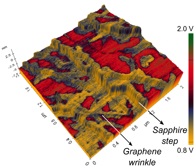
Figure 1: 3D overlay of the graphene topography, which displayed wrinkles and underlying sapphire steps as indicated, with the surface potential imaged via sideband KPFM.