|
Long days at offices and conference halls call for beer—
—and the only thing better than beer is FREE beer.
Visit our office on Thursday, July 21, 2016 from 5pm - 7pm as we serve some craft brew, bites to eat, and some friendly chatter as we all catch up on our work at the nanoscale and atomic force microscopy (AFM)!
Park Systems
3040 Olcott Street
Santa Clara, CA 95054
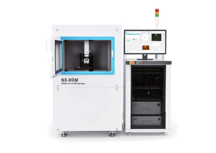
Park NX-HDM, one of several automated AFM tools from Park System.
Semiconductor device dimensions will be reaching the sub-1X nm node within a few years. Faced with this inevitability, researchers and manufacturers must have the capability to meet tougher metrology challenges calling for greater performance in resolution, precision, and accuracy as never required before.
The best tool for this job? Automated atomic force microscopy (AFM).
Automated AFM from Park Systems provides researchers and engineers a path to dramatically increase the throughput of their nanoscale data acquisition and analysis tasks. Whether it be device topography imaging for wafer-level device fabricators, roughness uniformity data for bare silicon wafer manufacturers, or critical dimension measurements for wafer design researchers, automated AFM will accurately, quickly, and repeatedly deliver unparalleled metrology data.
Join us as we introduce you to automated AFM from Park Systems—
the world's best solution for high-throughput nanoscale metrology challenges.
|