


Park Systems presents Nanoscale Solutions for Design and Manufacturing of Electronic Devices – a digital workshop series
This focused workshop series will provide an opportunity to Design, Process, Metrology, Yield and Failure Analysis Engineers to interface directly with Park Systems’ advanced applications experts and discuss day-to-day nanoscale solutions that address device manufacturing challenges.
Nanoscale Solutions for Design and Manufacturing of Electronic Devices – a digital workshop series
Register for the first workshop , held on June 25th
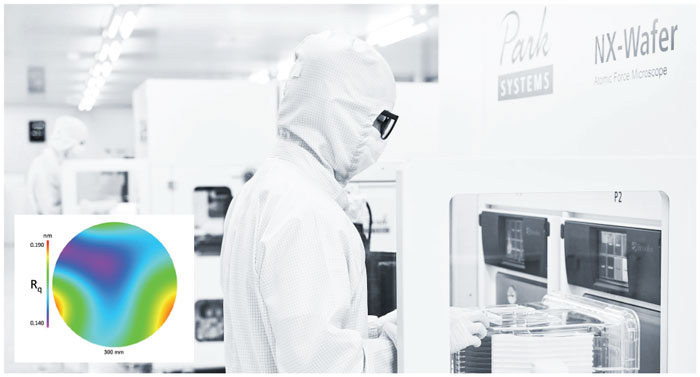
WHY PARK SYSTEMS ATOMIC FORCE MICROSCOPES
- • Leader in Automated AFM Equipment
- • Industry's sole non-destructive inspection and metrology technology, bundled in a single instrument
- • Lower in-fab costs compared to individual inspection or metrology tools
- • Fully-automated fleet matching tools enable day-to-day solutions for manufacturing yield challenges
- • The choice of many of the top 20 Semiconductor Manufacturers
WHY PARK SYSTEMS ATOMIC FORCE MICROSCOPES
- • Device Scaling and Novel Structure Designs
- • Process Advancements to Enable High Volume Manufacturing Solutions
- • Inspection and Metrology Methods to Capture Yield Excursion
- • Packaging and Reliability Considerations.
Q2CY20 Session: Nanoscale Solutions for Design and Manufacturing of Electronic Devices
Thursday, June 25, 2020
2 p.m. ET / 11 a.m. PT
Enhancing Detection Capabilities of AFM
Presented by Babar Hussain, Intel Corporation
Babar Hussain, PhD is a process engineer at Intel Fab 11x where he has a leading role in metrology support to different projects related to silicon photonics. He has over a decade of experience in research, development and manufacturing related to optics, electronics, and semiconductor device fabrication and characterization. His research has been published in more than 30 papers. He will discuss some of the technical challenges related to AFM's enhanced detection in the field of Silicon Photonics and Thin Film Metrology.
Automated AFM Technologies Addressing Yield Challenges
Presented by Dr. Doru Florescu, Park Systems
Doru Florescu, PhD has more than twenty years of experience in process and analytical capital equipment manufacturing for the semiconductor, storage and LED industries. He has been featured in over 40 publications and is currently working in the area of business development at Park Systems, the leading supplier of AFM to the semiconductor industry. Park’s inline AFMs are used widely by almost all of the top semiconductor manufacturers for automated defect review and they have an ongoing joint development program with imec to develop new protocols designed to increase production yield and device performance for the semiconductor industry. His talk will focus on how Park automated AFMs increases yield and performance for semiconductor device manufacturers.
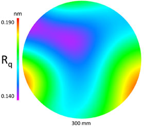
Surface Roughness * Trench In-line AFM Introduction * Wafer Edge Metrology
In the first session of the digital user workshop series, Park Systems industrial support team will discuss resolving existing challenges while further pushing the envelope on performance and cost of ownership for Semiconductor Device Manufacturing.