


Yueming Hua, Cynthia Buenviaje-Coggins
Park Systems Inc. 3040 Olcott St. Santa Clara, CA 95054, USA
Yong-ha Lee, Jung-min Lee, Kyung-deuk Ryang, Sang-il Park
Park Systems Corp. KANC 4F, Iui-Dong, 906-10 Suwon 443-270, Korea
ABSTRACT
As the feature size in the lithography process continuously shrinks, accurate critical dimension (CD) measurement becomes more important. A new 3-dimensional (3D) metrology atomic force microscope (AFM) has been designed on a decoupled XY and Z scanner platform for CD and sidewall characterization. In this decoupled scanner configuration, the sample XY scanner moves the sample and is independent from the Z scanner which only moves the tip. The independent Z scanner allows the tip to be intentionally tilted to easily access the sidewall. This technique has been used to measure photoresist line patterns. The tilted scanner design allows CD measurement at the top, middle, and bottom of lines as well as roughness measurement along the sidewall. The method builds upon the standard AFM tip design resulting in a technique that a) maintains the same resolution as traditional AFM, b) can be used with sharpened tips for increased image resolution, and c) does not suffer from corner inaccessibility from large radius of curvature tips.
Keywords: AFM, critical dimension, LER, LWR, sidewall, roughness
1. Introduction
The atomic force microscope (AFM) is a high resolution imaging tool. AFM has been widely used in universities for research, and it has also been used in industry as a metrology tool. One of the main applications of AFM for metrology is height measurement. There are many different AFM height measurements. It could be a simple step height measurement, CMP dishing measurement, pole tip recession (PTR) measurement for hard disk read/write head [1], trench depth measurement, etc. AFM is also used for roughness measurements. Recently AFM has been used for angle measurement. Previously FIB-SEM was the main tool for angle measurement. With FIB-SEM, the sample is first cut with an ion beam (FIB), and then an image is taken of the cross section for the angle measurement with an electron beam (SEM). With AFM, the angle can be measured non-destructively with the angle determined from a series of scan lines. This creates an angle measurement technique which is faster, more accurate, and less costly than traditional angle measurements taken with FIB-SEM.
AFM has also been used for CD measurement and sidewall imaging. This is one of the most challenging applications for AFM. As the feature size in the lithography process continuously shrinks, accurate CD measurement becomes more important. Just as nano-roughness became significant with ultrathin films, the sidewall roughness becomes significant in determining the functionality of devices with extremely small features. Accordingly the sidewall increasingly influences the CD measurement and characterizing the CD of a structure becomes more critical on the nanoscale. Over the past few years, AFM has become a powerful tool for accurate nanometrology. However, because most operate in a top-down configuration, AFM has limited access to the sidewall; this is especially true when the sidewall angle is near or greater than 90 degrees. To overcome this obstacle, special “boot shaped” tips have been developed with sophisticated detection algorithms to image sidewalls laterally [2], but this method has limited resolution
Metrology, Inspection, and Process Control for Microlithography XXV, edited by Christopher J. Raymond,
Proc. of SPIE Vol. 7971, 797118 · ⓒ 2011 SPIE · CCC code: 0277-786X/11/$18 · doi: 10.1117/12.879545
due to the large radius of curvature of the tip and blind spots at feature corners where the tip does not have sufficient physical access. This usually results in a rounded profile for the sharp corners at the bottom of features.
A new 3-dimensional (3D) metrology AFM has been designed on a decoupled XY and Z scanner platform for CD and sidewall characterization [3].
2. Decoupled XY and Z Scanning System
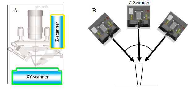
The new 3D AFM is based on a decoupled XY and Z scanning system [4]. In this decoupled scanning configuration, the XY scanner is a 2D flexure scanner. It moves the sample only in the XY direction and is independent from the Z scanner. The Z scanner is driven by a high force multi stack piezo element that moves the tip only in the Z direction (Figure 1-A). The independent Z scanner allows the tip to be intentionally tilted to easily access the sidewall (Figure 1-B). The tilted scanner design allows CD measurement at the top, middle, and bottom of the lines as well as roughness measurement along the line’s sidewall. The method builds upon the standard AFM tip design resulting in a technique that a) maintains the same resolution as traditional AFM, b) can be used with sharpened tips for increased image resolution, and c) does not suffer from corner inaccessibility from limited shape of tips with large radius.
 |
|
Figure 1, A. decoupled XY and Z scanning system; B, 3D AFM using tilting Z scanner
|
3. CD, LER, and LWR Measurement Using 3D-AFM
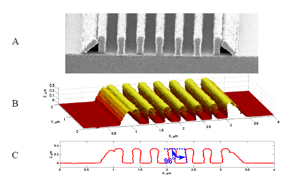
A 165 nm 1:1 line/space photoresist dense line pattern was imaged with 3D-AFM. The line height is about 330 nm and the aspect ratio is about 2:1. Figure 2-A shows the cross section SEM image of the pattern. It shows that the two lines at both ends of the pattern collasped and leaned onto the the lines next to them. Figure 2-B is the 3D-AFM image of the pattern. X direction is the AFM fast scan direction. It shows that 3D-AFM is able to image all the surfaces (top, bottom, and both sidewalls with undercut) of the pattern. The AFM image matches very well the SEM image. The AFM image also clearly shows the wavy structure of the sidewall that is created by the standing wave of the light used for the photoresist exposure. Even the cracks at the bottom of the collasped lines are very clear on the 3D-AFM image. Figure 2-C is a single line profile of the AFM image. The line profile matches with the SEM image very well and shows that the sidewall angle is about 96 degrees, which suggests the sidewall has about 6 degrees of undercut.
 |
|
Figure 2. A, cross section SEM image of the photoresist dense line pattern; B, 3D-AFM image of the pattern; C, AFM line profile of the pattern
|
 |
|
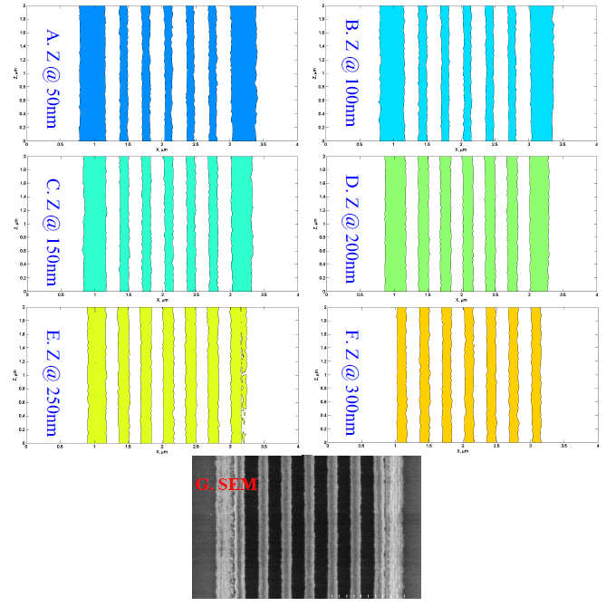
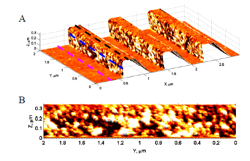
Figure 3. A-F, sliced 3D-AFM data at different Z heights; G, top-down SEM of the photoresist pattern
|
With the high resolution 3D-AFM data, we can slice the data at different Z heights to measure the contour of the pattern. This capability is unique to 3D-AFM. Figure 3 shows the contour of the pattern at different Z heights, from 50nm to 300nm. The colored regions of these sliced images represent the photoresist. The two wider lines at both ends are formed by the collasped lines. These sliced images clearly show the rough edges of the photoresist lines, which are very similar to what we can see from the top-down SEM image (Figure 3 G).
 |
|
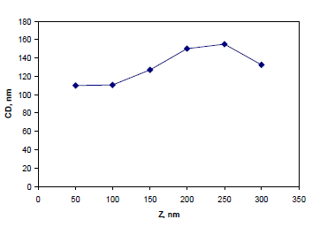
Figure 4. CD measurement at different Z heights
|
 |
|
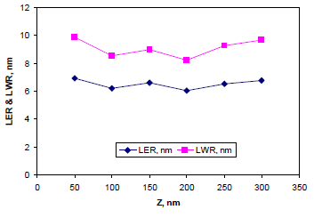
Figure 5. LER & LWR measurement at different Z heights
|
With the sliced 3D-AFM data, we can calculate the CD, line edge roughness (LER), line width roughness (LWR) of the lines at different Z heights. Figure 4 shows the measured line CD (average of the 5 photoresist lines in the middle). From the data, we can see the line width is narrower (110.2 nm) at the bottom, gets wider as the height goes up, reaches its maximum line width (154.9 nm) at about 250nm height, and then decreases.. This trend of the line width change is consistent with the profile observed from the cross section SEM of the photoresist pattern (Figure 2-A). Figure 5. shows that LER and LWR do not vary with height. The LER is between 6.2nm and 6.9 nm, and LWR is between 8.6nm and 9.9nm.
4. Sidewall Imaging Using 3D-AFM
A 300 nm semi-dense photoresist was also imaged with 3D-AFM with the Y direction (along the photoresist lines) as the fast scan direction. The advantage of scanning along the photoresist lines is that we can use high pixel resolution along the line without compromising the imaging speed.
Figure 6-A shows a 3D-AFM image. Because this image was taken with the Z scanner tilted to the left, the tip can image the top, bottom, and left sidewall of the pattern, but the right sidewall can not be imaged. The roughness image (topography image flattened by 1st order line-by-line in Y direction) is overlaid on the topography image to show the detail of the photoresist sidewall. The image shows that all three lines have similar sidewall roughness, and that the sidewalls are much rougher than the top and bottom surfaces. Figure 6-B is a direct view of the sidewall. This image clearly shows the grainy structure of the sidewall surface.
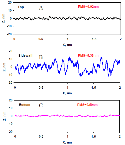
High resolution line profiles can be extracted from the 3D-AFM sidewall image. Figure 7 shows single line profiles at the different locations indicated in Figure 6-A. The roughness at the different surfaces (top, bottom, and side) can be measured with these line profiles. The measured roughness is 0.50 nm for the bottom surface, 0.92 nm for the top surface, and 5.38 nm for the sidewall surface of the photoresist line. The measured sidewall roughness is directly related to the LER of the line.
 |
|
Figure 6. A, 3D-AFM image of a 300 nm semi-dense photoresist line pattern showing the detail of the sidewall; B, a
direct view at the sidewall showing the grainy structure of the sidewall surface |
 |
|
Figure 7. AFM line profiles at different surfaces shown in Figure 6A as dotted lines: A, top surface of a photoresist
line; B, sidewall of a photoresist line; C, bottom surface of the sample |
5. Conclusions
This new 3D AFM is capable of advanced 3D imaging of both isolated lines and dense line patterns. The tip can easily reach the undercut sidewall and sharp corner at the bottom. This 3D AFM can be used for CD, LER, LWR, and sidewall roughness measurement. 3D-AFM is an excellent complementary technology for CD-SEM and FIB-SEM.
Acknowledgement
We would like to thank Dr. Jane Frommer and Ms. Linda Sundberg at IBM Almaden Research Center for providing samples and helpful discussion.
References
[1] Joonhyung Kwon, Yong-Seog Kim, Kwanseok Yoon,Sang-Min Lee, Sang-il Park, Advanced nanoscale metrology of pole-tip recession with AFM", Ultramicroscopy 105, 51?56 (2005)
[2] Bharat Bhushan, Harald Fuchs, and Masahiko Tomitori, Applied Scanning Probe Methods VIII,Springer, 31-75 (2008)
[3] Sang-Joon Cho, Jung-Min Lee, Byung-Woon Ahn, Joonhui Kim, Young Yoo, Yueming Hua,Sang-il Park, “Three-dimensional imaging of undercut and sidewall structures by atomic force microscopy”, Review of Scientific Instruments, 82, 023707 (2011)
[4] Joonhyung Kwon, Jaewan Hong, Yong-Seok Kim, Dong-Youn Lee, Kyumin Lee, Sang-min Lee,Sang-il Park, “Atomic force microscope with improved scan accuracy, scan speed,and opticalvision”, Review of Scientific Instruments 74, 4378-4383 (2003)