


What is a Good AFM?

When purchasing an AFM, it is important to evaluate it as a whole. There are several features that could be important depending on the final system application. Before making a purchase, you should ask yourself the following questions:
- Is the system designed for industrial or research applications?
- Is the system going to be installed in a multi-user facility?
- Will the system support all of the available options that I need?
- Is the system easy to use for low-level users? Is the AFM powerful enough for high-end users?
Once these questions have been answered, and a list of viable systems has been compiled, the user needs to make a fundamental comparison of the units that best meet their requirements.
In order to help you with this process, we’ve put together a comprehensive overview of what makes a good AFM.
The Basics
Historically AFMs have proven themselves reliable instrument for determining relative sample dimensions but have struggled to provide accurate absolute dimensions of surface features. As the dimensions found in research and industrial applications become smaller and smaller, it is now more important than ever for AFMs to measure the absolute dimensions of surface features with accuracy and repeatability.
For taking nanoscale measurements, the accuracy and reliability of measurements and the flexibility of available modes and options are just as important as resolution.
AFM performance is influenced by the following seven attributes:
- Noise Floor
- XY Scan Flatness
- Tip Life
- Thermal Drift
- Available SPM Modes
- Option Compatibility
Noise Floor
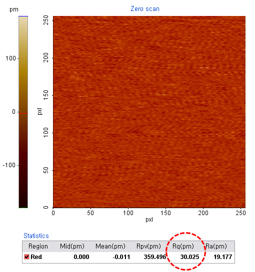
Even the smallest environmental vibrations can add noise to AFM results, making it a challenge to image very small details and characterize the flattest surfaces. To measure the baseline noise, or noise floor, the user brings the cantilever to the sample surface and obtains the system response to a "zero scan" (See Figure 1). A good AFM should be isolated from vibrations to achieve a noise floor below 0.5A
- 0 x 0 nm scan, staying in one point
- 0.5 gain, in contact mode
- 256 x 256 pixels
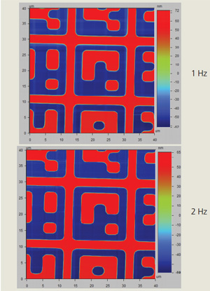
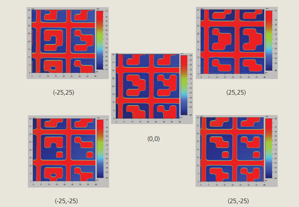
XY Scan Flatness
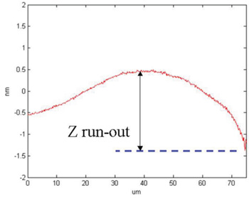
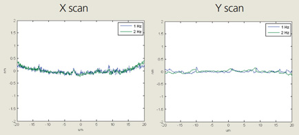
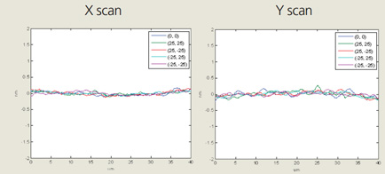
A customer must look for a scanner design which minimizes out-of-plane motion when imaging a flat surface. A good AFM scanner must keep the Z out-of plane motion within a few nanometers over the entire scan range, independent of scan rate (see Figure 3), scan size, and scanner offset (see Figure 4).
XY Scan Linearity
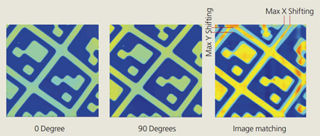
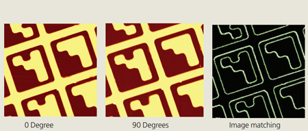
The XY scan linearity is another important feature that affects the accuracy of the imaging results an AFM can provide. If the X and Y scan movements are coupled, as in a tube scanner, an extension in the X direction will directly influence the scanner’s Y position. The XY scan linearity is measured using two orthogonal scans and subsequent image matching as shown in Figure 5. The amount of mismatch in two images taken by the scanner will reveal how linear its X and Y scan movements are.
To get the best results, customers should look for a scanner design which maximizes the XY scan linearity. A good AFM scanner must keep the XY scan linearity less than 0.05% at a random coordinate (see Figure 6), independent of scan rate (see Figure 7) , scan size, and scanner offset (see Figure 8).
Tip Life
Tip life is an important factor in getting high-quality images with consistency and reliability. When the tip touches the sample and becomes blunt, it limits the resolution of the AFM and reduces the quality of the image. For softer samples, tip-surface contact damages the sample as well as the tip, compounding the inaccuracies of sample height measurements. Consequently, preserving tip integrity enables consistent high-resolution and accurate data.
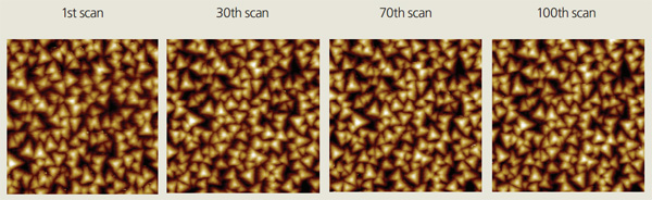
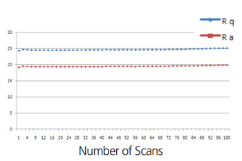
A good way to test the tip life of an AFM system is by imaging CrN, which has sharp and pointy features on a very hard surface. If a tip becomes blunt or damaged, it can no longer reach the bottom of the features, and the images become blurred.With a good AFM, the sharpness of the tip can be preserved even after 100 image scans of the CrN sample as shown in Figure 9, while maintaining the same sample surface roughness (see Figure 10).
Thermal Drift
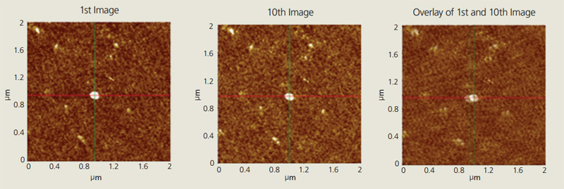
An AFM tip may experience undesired motion due to the thermal expansion or contraction of mechanical parts within the instrument. This undesired motion, called thermal drift, must be minimized to accurately image samples smaller than 1 μm. The drift rates in the X and Y directions are determined by marking the locations of characteristic structures on the sample surface and measuring deviations from these points after several scans. A good AFM has a drift rate smaller than 1.5 nm/minute/oC.
Available SPM Modes
Today’s AFMs can characterize a wide range of physical properties, depending on the specific sample and application needs of the customer. Of particular importance are the SPM modes which probe the following properties:
- Standard imaging
- Chemical properties
- Dielectric/piezoelectric properties
- Force measurement
- Electrical properties
- In-liquid imaging
- Magnetic properties
- Mechanical properties
- Optical properties
- Thermal properties
When purchasing an AFM, pay careful attention to which SPM modes it supports.
Option Compatibility
A good AFM must provide a wide range of option compatibility in order to facilitate data acquisition in a wide variety of conditions and sample environments. Of particular importance are:
- SLD (Super Luminescence Diode) light source for low coherence
- Z scanner with scan range of 25 microns
- Heating & cooling sample stage
- Liquid cells
- Live cell chamber
- Motorized XY sample stage
- Signal access module
- Step and scan function for automatic sequential imaging
- Tunable magnetic field generator