


John Paul Pineda, Gerald Pascual, Byong Kim, and Keibock Lee
Technical Marketing, Park Systems Inc., Santa Clara, CA, USA
Introduction
Semiconductor devices are the foundation of modern electronics due to their importance in the function of electrical circuitry with components such as transistors, diodes, and integrated circuits. These devices have become ubiquitous in a wide range of applications. The most common of which are the design and manufacture of 1) common analog appliances such as radios and 2) digital circuits for use in computer hardware. [1] Key electrical parameters such as dopant concentration level, carrier type, and defect densities are fundamental factors that influence the performance of semiconductor devices. Thus, a technique that can measure these characteristics and investigate samples with nanoscale features must be utilized in evaluating device reliability. There are several methods for the characterization of semiconductors. Examples include Scanning Electron Microscopy (SEM), Transmission Electron Microscopy (TEM), Secondary Ion Mass Spectroscopy (SIMS), Electron Beam Induced Current (EBIC) and one-dimensional Capacitance Voltage (C-V), among others [2]. However, some of these methods are destructive, others have laborious sample preparation requirement, and others still do not effectively determine two-dimensional quantities of sub-device scale. The need for nextgeneration characterization tools was driven by these shortcomings as well as the realization that ever-smaller device geometry and high reliability requirements were beginning to trend within the industry. To satisfy this new degree of difficulty in the metrology of semiconductor device processes, various types of scanning probe microscopy (SPM) have been deployed to meet the challenge. Scanning Capacitance Microscopy (SCM) and Kelvin Probe Force Microscopy (KPFM) combined with Atomic Force Microscopy (AFM) are the most powerful methods for characterization of semiconductor devices because of their non-destructive scanning ability, accuracy in measurements of samples with nanoscale features, and the lack of any sample preparation. In addition, the integration of these methods with AFM enables it to acquire both topography and electrical property data simultaneously without changing the sample or tip. To this end, SCM and KPFM were used to investigate an SRAM device and the data shows that these techniques are effective means for the electrical properties characterization of semiconductor devices.
Experiments
An SRAM sample [3] was investigated using a Park NX20 AFM system [4]. The electrical properties of the sample were characterized under ambient air conditions using two different techniques: SCM and KPFM. A cantilever with a metal-coated tip was utilized in both techniques.
In SCM [5], the sample topography is collected using contact mode AFM simultaneously with capacitance imaging all in a single scan. The electrical properties of the sample are measured from the variation in radio frequency (RF) amplitude signal due to changes in capacitance between the tip and the sample. The hardware configuration of this mode consists of several modules including the cavity resonator, frame module, SCM probehand, SCM sample holder, and an SCM cantilever chip with a connected probe wire. The SCM probehand was connected to an RF sensor, comprised of the cavity resonator and frame module, to detect the change in capacitance between the probe tip and the sample during scanning. The frame module generates and amplifies the driving signal which oscillates the resonator during SCM measurements. The cavity resonator transforms the capacitance change between the probe tip and the sample into an RF signal. The resonant frequency of the resonator is proportional to 1/√ LC, where L is inductance of the resonator, and C is the capacitance. For this study, a resonance RF curve with a peak of 697.8 MHz was used (see Figure 1). This curve is steepest at an operating resonant frequency of 705.4 MHz. This is the point on the curve where changes in amplitude due to frequency shifts, induced by tip-sample capacitance changes, would be most easily observed.
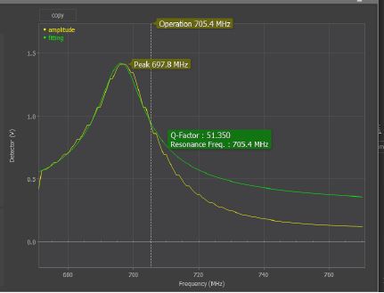 Figure 1. Resonance RF curve displaying the SCM detector signal (V) versus frequency (MHz). The optimal frequency to oscillate the resonator to achieve the highest detection sensitivity in SCM imaging is 705.4MHz.
The output signal from the resonator is monitored and coupled with a lock-in technique to acquire the final capacitance map reported here. In this experiment, a lock-in amplifier, embedded internally in the NX electronics, with an AC voltage frequency of 17 kHz was selected after optimizing the scan parameters for acquiring topography data. Parameters for SCM imaging were also optimized by closely monitoring the SCM signal. The AC bias amplitude selected was 1 V, while for AC bias, the phase chosen was a 0° reference phase. A second order filter with a 1 ms time constant was also selected for monitoring the output signals. A sensitivity value of 1 V was set to remove unwanted noise in the signals.
In KPFM mode, there are two interaction forces between the AC biased tip and the sample: the electrostatic force and Van der Waals force. The Van der Waals force is harnessed to generate the sample's surface topography while the electrostatic force between the tip and sample generates data for the sample's electrical properties. The obtained cantilever deflection signal contains both sets of information; therefore, a method that can completely separate these signals is the key to successful imaging. There have been methods introduced to accomplish this, one of which is two-pass scanning. However, this method is two times slower than typical AFM imaging as two separate scans need to be conducted. In the Park NX20, lock-in amplifiers embedded its electronics are used to separate signals. This allows for the acquisition of both topography and EFM data in a single-pass scan. Two amplifiers are used by the system, named lock-in 1 and lock-in 2. Lock-in 1 obtains the topography information by analyzing the tip motion caused by the Van der Waals interaction, while lock-in 2 obtains electrical property information by analyzing the frequency of the applied AC voltage signal to the tip which, in turn, generates an electrostatic force interaction with the sample. The frequency of the applied AC voltage signal is chosen to be smaller (~17 kHz) than the cantilever oscillation frequency (70- 330 kHz), enough so that the two signals do not interfere each other [6]. In this experiment, lockin 2 with an AC voltage frequency of 17 kHz was selected after optimizing scan parameters for topography data acquisition. Furthermore, a separate DC bias was applied to the cantilever and controlled for to create a feedback loop that would zero out the electrical oscillation between the tip and the sample caused by the application of an AC bias to the cantilever. The value of this offsetting DC bias that zeroes out the AC bias-induced electrical oscillation is considered to be a measure of surface potential [6, 7].
RESULTS & DISCUSSIONS
The region of interest in this investigation is in the sample's NMOS region. The acquired images from each technique were analyzed using XEI software developed by Park Systems which mapped the acquired signals to a color table. The topography data acquired in both techniques clearly show the NMOS region but no significant information related to the type and level of dopant concentration. This is in contrast with the electrical property data acquired in each mode showing not only the NMOS structure, but also the type and level of doping concentrations across the sample.
Figure 2, shown below, is the topography and SCM measurement of the SRAM sample with regions of different doping levels from 2x1016 cm-3 to 2x1020 cm-3. The SCM image clearly shows various regions doped with different types of dopants and at varying concentration levels. The various steps in the color gradient are particularly helpful with observing concentration levels as several regions on the device show various shades of bright (p dopant presence) and dark (n dopant presence) color mapping. The intensity of the shading correlates to the degree with which those regions are doped with extremely bright and dark areas having the lowest and highest dopant concentration levels. For example, the device's p-channel with a doping level of 1x1017 cm-3 is clearly visible in the SCM image. The narrow regions of the p-channel approximately 100 nm wide show the separation of regions with alternating dopant types in the configuration of a typical NPN transistor. Furthermore, the resolution of SCM is high enough to show multiple darker spots present in what device fabricators intended to be a continuously solid bright line of positively doped material on the left side of the device. Characterizing electrical properties with this level of detail can be key in understanding the functionality of a semiconductor device.
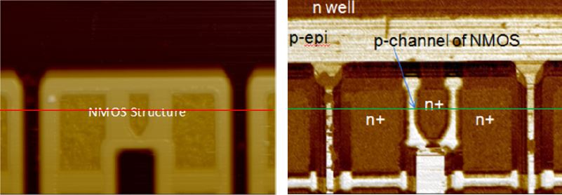
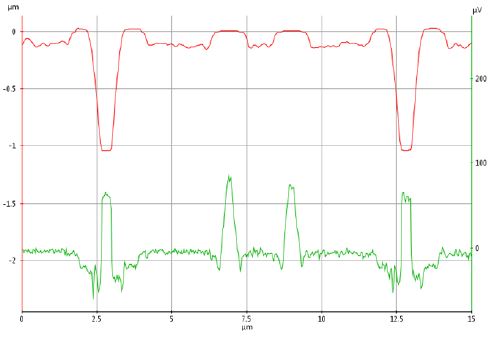
Figure 2. Topography (top-left) and SCM (top-right) data acquired from the sample device. Topography line profile (red line, y-axis on left) and SCM line profile (green, y-axis on right): Doping level: p-epi (2x1016 cm-3), n well (2x1017 cm-3), p channel (1x1017 cm-3) , n+ contacts (2x1020 cm-3).
As with the SCM and topography images, the corresponding line profiles generated after scanning can also yield significant insight into the design of the device. Here we first consider the line profile for the topography data indicated in red on Figure 2. When compared to the SCM image with the device features labeled, one can see that each NPN transistor device is separated from the next by boundaries nearly 1 μm in depth with high levels of positive dopant concentration. The edges of each boundary are bordered by a slightly raised area of about 0.1 μm. If one were to overlay this topography data onto the SCM image, the edges of each boundary can be seen to have lower dopant concentration (darker color) than the n+ contacts making up the NPN transistors. This is further supported by the line profile of the SCM data (green line on figure 2) where the regions immediately before and after the boundaries (which again, feature large decreases in positive dopant concentration) are measured at slightly more negative μV levels (-30 μV) than the rest of the negatively doped portions (-10 μV) of the device shown in the SCM image. An additional observation can be made in the central portion of the area of interest where p-channels of an elevated height around 0.1 μm can be detected perpendicular to the p-epi region of the device. These central p-channels have a relatively lower concentration of positive dopant (approaching 80-90 μV) where they are seen bright along the both green line in the SCM image as well as in the image as a whole.
While SCM provides excellent topography and electrical property data with high spatial resolution, it is a technique that is enabled through the purchase of additional hardware from many microscopy vendors. Furthermore SCM must be performed using contact mode AFM which results in the consumption of probes at an accelerated pace compared to non-contact mode AFM. In situations limited by hardware availability or fiscal considerations, electrical characterization of semiconductor devices can still be performed at a diminished, yet viable manner using KPFM, a surface potential measurement technique. Although not as effectively detailed, KPFM can provide researchers with images and data comparable to that acquired with SCM. Both techniques can characterize the structure of the device and reveal the dopant concentrations in various regions across the area of interest. Areas with negative dopant concentrations are again presented as darker areas and those with positive dopant concentrations are shown to be brighter. The key differences between the two techniques are that of lateral resolution and dopant detection sensitivity. Comparing the SCM image with the KPFM image, one can see the p-channels of the device are much wider when observed in KPFM. One possible explanation of this difference is that KPFM is designed to see potential over an entire sample surface whereas SCM makes direct contact with the sample surface to detect capacitance responses. An alternative explanation would be that KPFM can be influenced by charges in the ambient air around the tip as well as in moisture that has adhered to the sample, both of which are possible sources of alterations in charge distribution. SCM on the other hand has the tip engage the surface of the tip directly, penetrating through any possible moisture layer, creating a point of direct contact which is less likely to be affected by parasitic charges from the scanning environment.
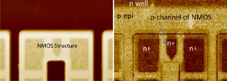 Figure 3. Topography (left) and KPFM (right) data acquired in KPFM mode.
p-epi (2x1016 cm-3), n well (2x1017 cm-3), p-channel (1x1017 cm-3), n+ contacts (2x1020 cm-3).
Summary
The topography and electrical properties of an SRAM sample have been characterized using SCM and KPFM with a Park NX20 AFM system. The data collected in this investigation reveals that both techniques can provide qualitative and quantitative information for electrical characterization of semiconductor devices. The results demonstrate that SCM provides greater lateral resolution and higher contrast mapping of electrical properties, including dopant type and level of concentration, when compared to KPFM. However, KPFM remains an effective source of data that can be used to reach similar conclusions about a sample under investigation as SCM. Overall, the techniques described in this study will successfully provide researchers and device engineers with key electrical parameters information to better evaluate the device reliability and monitor semiconductor device processes at nanoscale level.
REFERENCES
[1] M. Deen, et al., Electrical Characterization of Semiconductor Materials and Devices. Springer Handbook of Electronic and Photonic Materials, pp 409-438
[2] D. Schroder, Semiconductor Material and Device Characterization. 3rd Edition, Wiley Interscience, Chemical and Physical Characterization, pp 627-659
[3] SCMSAMPLE. (n.d.). Retrieved June 20, 2016, from http://www.brukerafmprobes.com/a- 3553-scmsample.aspx
[4] Park NX20 Atomic Force Microscope. (n.d.). Retrieved June 13, 2016, from http://www.parkafm.com/index.php/products/research-afm/park-nx20/overview
[5] Park SCM Technique: http://www.parkafm.com/index.php/park-spm-modes/94-electricalproperties/ 235-scanning-capacitance-microscopy-scm
[6] Park AFM Modes and Techniques. (n.d.). Retrieved June 13, 2016, from http://www.parkafm.com/index.php/park-afm-modes
[7] W. Melitz, et al., Kelvin probe force microscopy and its application, Surface Science Reports 66 (2011) 1–27, pp 2-4
APPENDIX
Electrostatic Force Microscopy (EFM) was also used as a third means of characterizing the electrical properties of the SRAM sample. A short discussion of the setup for this technique and the data acquired with it follow below.
EFM follows the same configuration as KPFM wherein lock-in amplifiers were used to acquire both topography and EFM data using non-contact AFM in a single scan. The difference in EFM is that there is no feedback loop which constantly zeroes out the AC bias of the collected frequency signal. Scan parameters in EFM were nearly identical with what was used in KPFM with the notable of exception of the servo gain no longer needing to be optimized at a value of 7 after monitoring the tip bias signal.
An additional alternative to SCM for electrical property characterization is EFM. Here, instead of separate signals for topography and capacitance/surface potential data, EFM instead acquires amplitude and phase signals. The amplitude signal reflects the degree to which an area of the sample has been doped. In Figure 4 below, the EFM amplitude image on the left shows the n+ contacts and n well region of the device in brighter colors as they have relatively higher dopant levels (2x1020 cm-3 and 2x1017 cm-3 respectively) than areas such as the p-epi which have lower dopant levels (concentrations of 2x1016 cm-3) and are shown to be darker. Polarity of the dopants in each region can be confirmed by the EFM phase image which again shows negatively doped regions of the device with brighter colors and positively doped regions in darker shades.
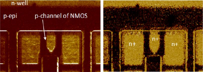
Figure 4. EFM amplitude (top-left), EFM phase (top-right), p-epi (2x1016 cm-3), n well (2x1017 cm-3), pchannel (1x1017 cm-3), n+ contacts (2x1020 cm-3).