


2017 SPIE Advanced Lithography Luncheon

Park Systems visits downtown San Jose to hold a luncheon alongside the 2017 SPIE Advanced Lithography conference. After the world's premier lithography event kicks off its programming on Monday, February 27, join us just a block away from the San Jose Convention Center at Morton's The Steakhouse for lunch and to learn about the latest advances in nanoscale characterization for the semiconductor industry
• Event Date and Time : Monday, February 27 — 12:00p to 2:00p
• Venue : Morton's The Steakhouse — San Jose, CA (Map)
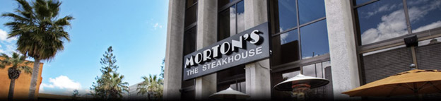 Morton's The Steakhouse, San Jose
The featured speaker at the luncheon will be Dr. Ardavan Zandiatashbar, Technical Accounts Manager at Park Systems. Dr. Zandiatashbar will speak about the advances Park has made to atomic force profiler (AFP) design and the benefits these next-generation tools have in tackling the challenges faced by foundries today.
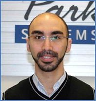 Dr. Ardavan Zandiatashbar
Technical Accounts Manager, Park Systems
Automated AFM for Small-Scale and Large-Scale Surface Profiling in CMP Applications
As the feature size is shrinking in the foundries, the need for inline high resolution surface profiling with versatile capabilities is increasing. One of the important areas of this need is chemical mechanical planarization (CMP) process. We introduce a new generation of atomic force profiler (AFP) using decoupled scanners design. The system is capable of providing small-scale profiling using XY scanner and large-scale profiling using the slider. Decoupled scanners design enables enhanced vision which helps minimizing the positioning error for locations of interest in case of highly polished dies. Non-Contact mode imaging is another feature of interest in this system which is used for surface roughness measurement, automatic defect review, and deep trench measurement. Examples of the measurements performed using the atomic force profiler is demonstrated.
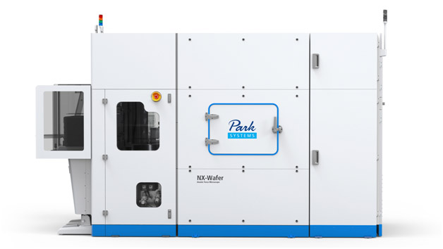 Park NX-Wafer
Low Noise, High Throughput Atomic Force Profiler with Automatic Defect Review
About SPIE
SPIE, the international society for optics and photonics, was founded in 1955 to advanced light-based technologies.
Serving more than 264,000 constituents from approximately 166 countries, the not-for-profit society advances emerging technologies through interdisciplinary information exchange, continuing education, publications, patent precedent, and career and professional growth.
SPIE annually organizes and sponsors approximately 25 major technical forums, exhibitions, and education programs in North America, Europe, Asia, and the South Pacific.
In 2016, SPIE provided $4 million in support of education and outreach programs.
SPIE publishes the SPIE Digital Library, containing more than 450,000 research papers from the Proceedings of SPIE and the Society’s 10 scholarly journals with around 18,000 new papers added each year, and more than 260 eBooks from the SPIE Press catalog. The SPIE Press publishes print monographs, tutorial texts, Field Guides, and reference books. SPIE also publishes a wide variety of open access content.
Membership includes Fellows and Senior Member programs. The Society has named more than 1,000 SPIE members as Fellows since 1955, and implemented its Senior Member program in 2008.
The SPIE awards program serves to recognize outstanding contributions from individuals throughout the scientific community.
The SPIE international office is located Bellingham, Washington and the SPIE Europe office is located in Cardiff, Wales.
• Link : http://spie.org/conferences-and-exhibitions/advanced-lithography