


2D Moiré Superlattice Electromechanical Characterization with Piezo-response Force Microscopy
Byong Kim, John Paul Pineda, Ben Schoenek, Jiali Zhang, Armando Melgarejo, Research Technical Services, Park Systems, Inc., USA
Qiong Ma, Department of Physics, Boston College, USA
Ilka Hermes, Applications, Park Systems Europe GmbH., Germany
Dae Yoen Won, Research & Development, Park Systems Corp., Korea
Introduction
Stacking two-dimensional (2D) materials within the van der Waals interaction distance of each other can generate long-range wavelength ordering called Moiré superlattice periodicity. In the case of graphene on hexagonal boron nitride (hBN), for example, this effect would appear on the top layer of graphene and cause the energy bandgap of graphene to open [1-3]. By regulating the lattice orientation between graphene and boron nitride, one can vary the Moiré periodicity's wavelength, thus tuning the graphene energy bandgap. The energy bandgap range impacts graphene’s device functionalities and performance [4]. Therefore, it is useful for researchers to have a simple way of deciphering the Moiré shape and periodicity, especially when designing 2D graphene/BN-like heterostructured materials and devices.
Piezo-response Force Microscopy (PFM) is a contact Atomic Force Microscopy (AFM)-based imaging technique. It is widely used for electromechanical mapping of a sample with nanoscale lateral resolution and has shown promise in detecting local strain gradients and piezoelectricity in various 2D heterostructured material systems, including graphene/hBN [5]. In this paper, we use contact resonance PFM to characterize the Moiré shape and periodicity–the superlattice wavelength. Using two types of graphene-on-hBN stacked systems, we correlate these variables to describe lattice misalignment and rotation.
Experiment and Result
(a) Monolayer graphene on hexagonal boron nitride
The sample is a monolayer graphene epitaxially grown on a hexagonal boron nitride. PFM setup uses a Park NX10 AFM system coupled with a Zurich Instruments HF2 lock-in amplifier [6]. The PFM cantilever probe (PPP-EFM) used is a ~3 N/m Si cantilever probe, PtIr-coated, with an air resonance ~75 kHz. The AC voltage applied is 2 V, and the contact resonance frequency used is ~330 kHz. The AFM loading force applied during PFM scanning is 40 nN, and the PFM scan rate is 1-1.5 Hz. The 100 nm x 100 nm and 200 nm x 200 nm scan size data were acquired. To perform the contact resonance PFM on the graphene sample, we followed the procedure outlined by Hermes et al., who used PFM to image ferroelectric domains in Bismuth Ferrite (BFO) [6], with the following exception. In the reported PFM study on BFO, surface pits prevented the contact resonance frequency from staying within acceptable levels during scanning. Thus, it was necessary to enable “Double Frequency Resonance Tracking” (DFRT)’s PID control during scanning to compensate for shifts in contact resonant frequency. However, in this report, the topography of graphene/hBN in the scanning area is atomically flat and virtually featureless. Thus, there is a negligible contact resonance frequency shift during the PFM operation, which allows for high-resolution PFM data without enabling DFRT's PID control.
Figure 1(a) is a contact-resonance PFM amplitude image that shows a honeycomb Moiré periodicity. The periodic superlattice spacing is 15 nm, two orders of magnitude larger than the atomic lattice constants of graphene and hBN. For aligned graphene on boron nitride, a Moiré periodicity ~14-15 nm is expected [2,3]. Our results are consistent with this value. When zoomed out to 200 nm x 200 nm and scanned again, the sample shows a consistent 15 nm periodicity and a coherent piezo-response signal, as shown in Fig. 1(b).
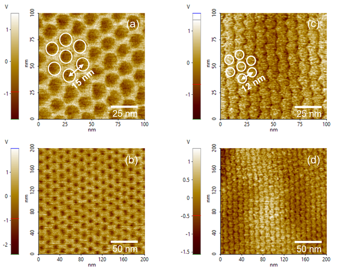
Figure 1. PFM amplitude images. Honeycomb Moiré patterns with periodicity 15 nm on monolayer graphene/hBN (a) and (b), and with periodicity 12 nm on twisted bilayer graphene/hBN (c) and (d).
(b) Twisted bilayer graphene on hexagonal boron nitride
The sample was prepared by employing an exfoliation technique and purposely misaligning the upper graphene bilayer graphene by 1.15 degrees to the underlying hBN substrate. The surface of the exfoliated bilayer graphene was studied with noncontact AFM survey imaging, and a residue film with a nanometer-scale thickness, likely leftover from the exfoliation process, was covering the exfoliated sample surface. First, a PPP-EFM probe scanned the sample in contact mode AFM (applying up to ~500 nN loading force) to sweep aside the residue. Next, a new PPP-EFM probe performed PFM measurements on the cleaned bilayer graphene surface. The PFM setup and imaging procedures used for the twisted bilayer graphene characterization are the same as that of the monolayer graphene PFM study, except for the following parameters. The AC voltage applied is 6 V, and the contact resonance frequency used is 354 kHz. The AFM loading force applied during PFM scanning is 500 nN, and the PFM scan rate is 2-3 Hz.
Figure 1(c) is a 100 nm x 100 nm scan contact-resonance PFM amplitude image. One can outline a hexagonal pattern and determine the twisted bilayer's superlattice periodicity to be 12 nm. There is a 20% difference in Moiré periodicity between bilayer graphene and monolayer graphene, with the latter being larger. The 12 nm wavelength periodicity should correspond to the bilayer graphene's configuration misaligned by the 1.15-degree twist on BN. Monolayer graphene with 15 nm periodicity represents monolayer graphene on hBN without misorientation between two layers. This observation agrees with the general understanding that the Moiré periodicity, i.e., the superlattice wavelength, is reduced further as the top adlayer is increasingly misaligned to the underlying layer [7]. Fig 1(d) is the PFM amplitude data of the same area after zooming out to the 200 nm x 200 nm scan area. The individual component that makes up the honeycomb array is discernable everywhere with the same periodicity in the zoomed-in and zoomed-out scan images of Figs 1(c) and (d).
Summary
Moiré superlattice periodicity in two types of graphene on hexagonal boron nitride structures is characterized by contact resonance PFM. Bilayer graphene misoriented with a 1.15-degree twist on hBN showed a 12 nm Moiré wavelength periodicity, which is 20 % smaller than the 15 nm lattice periodicity for monolayer graphene on hBN. The formation of a Moiré superlattice with a wavelength of 14-15 nm is the signature of aligned monolayer graphene on hBN. Therefore, contact resonance PFM is a suitable instrument for performing quality control and distinguishing the Moiré periodicity in graphene/hBN-like 2D multilayered samples.
Acknowledgment
The authors thank Prof. David Goldhaber-Gordon’s group from Stanford University for providing the epitaxially-grown monolayer graphene/hBN sample.
References
1. S. Tang et al., Scientific Reports 3(2666) 2013.
2. C. Woods et al., Nature Physics 10 (2014) 451–6.
3. A. Zandiatashbar, B. Kim, Y. Yoo and K. Lee, Microscopy Today, Volume 23, Issue 6, November 2015, pp. 26 – 31.
4. Z. Zheng, Q. Ma et al., Nature, 588 (2020) 71-76
5. L.J. McGilly et al., arXiv:1912.06629 [cond-mat.mes-hall]
6. I. Hermes and R. Stomp, Park AFM Application Note: DFRT PFM. https://parksystems.com/images/media/appnote/DFRT-PFM_AppNote_Park-Systems.pdf
7. N. Neek-Amal and F. M. Peeters, Appl. Phys. Lett., 104 (2014) 041909