


Investigating the origin of the domain structure in the piezoresponse of hybrid perovskites
Ilka Hermes1
1Park Systems Europe, Germany
Introduction
Methylammonium lead iodide (MAPbI3), first described in 1987 and since 2009 successfully applied in photovoltaic (PV) devices,1,2 crystallizes in a tetragonal perovskite structure at room temperature.3 Because perovskite materials often feature ferroic properties and MAPbI3 additionally has a polar methylammonium center-ion (2.3 D),4 researchers have long discussed a possible ferroelectric and ferroelastic nature of the material.5-7
Ferroelectricity originates from a change in crystal symmetry during a ferroelectric phase transition, where the loss of the center symmetry causes a spontaneous electrical polarization. To lower the electrostatic energy the crystal forms domains of parallelly aligned polarization. Depending on the orientation of the domain polarization with respect to the walls between different domains, the walls can carry a bound charge. This charge can be compensated by free charge carriers leading to conducting 2D sheets.8 For MAPbI3, theoreticians suggested that alternatingly charged domain walls could act as charge-selective carrier pathways, lowering the recombination in the PV material.5
Ferroelasticity is a result of a change in the crystal system, e.g., from a cubic to a tetragonal structure during a ferroelastic phase transition. The distortion of the unit cell introduces an internal stress in the material that is reduced via the formation of domains with alternating unit cell orientations.8 The structural anomalies at the domain walls between ferroelastic domains can lead to a local loss of center symmetry and thereby cause a domain wall polarization.9 For MAPbI3, theoreticians proposed a similar effect, beneficial for directed charge carrier extraction.10
The characterization and classification of ferroelectric domains requires Piezoelectric Force Microscopy (PFM), a contact mode Atomic Force Microscopy (AFM) method, that resolves local electromechanical responses with a nanometer resolution.11,12 In PFM, a conductive tip attached to a cantilever scans the surface of a ferroelectric sample, while applying an AC voltage between the tip and a back electrode below the sample. Since all ferroelectric materials are piezoelectric, the applied AC voltage introduces a periodic deformation of the sample, called piezoresponse (Figure 1a). For domains with a polarization perpendicular to the sample surface, the piezoresponse is either in phase or 180° out of phase with the applied AC voltage, depending on the polarization orientation in the domains below the tip.11
In its standard configuration, PFM applies low frequency AC voltages. This technique, called off resonance PFM, is less prone to topographic crosstalk since it operates far from the cantilever’s contact resonance (3 - 5 times of the free resonance). However, materials with weak inherent piezoresponse or thin films, may require an increase of the signal-to-noise ratio by choosing an AC voltage close or at the contact resonance of the cantilever.11 While this single frequency resonance enhanced PFM technique improves the sensitivity to the piezoresponse, the detected signal now also becomes more susceptible to crosstalk, e.g., from topography and sample mechanics. The frequency of the contact resonance strongly depends on a stable and unchanged tip sample contact, which is difficult to achieve while scanning, particularly on samples with a lot of topography or heterogeneous nanomechanics as expected on domains with a ferroelastic nature.13
Here, Dual Frequency Resonance Tracking (DFRT), available by combining a Park Systems NX10 AFM with a Zurich Instruments HF2 Lock In Amplifier (see Application Note 56), allows differentiating between true electromechanical signal contributions and mechanical or topographic crosstalk using an additional feedback that tracks the contact resonance. For DFRT, the HF2 generates sidebands left and right of the contact resonance at frequencies given by the bandwidth at half maximum of the contact resonance (Figure 1b). During the PFM scan, the feedback continuously compares the amplitudes of both sidebands and readjusts the frequency of the AC voltage to keep the amplitude ratio constant. Thereby, DFRT not only facilitates a minimization of crosstalk, but also adds another signal channel for local visualization of the contact resonance distribution, which allows resolving mechanical heterogeneities qualitatively.13
In this application note, we imaged the piezoresponse on a MAPbI3 film via DFRT and resolved an out-of-plane domain with distinct PFM amplitude and phase signal as well as a correlating shift in the contact resonance frequency. The frequency signal shows a mechanical contrast between the domain and the bulk grain, suggesting a ferroelastic character of the domain.
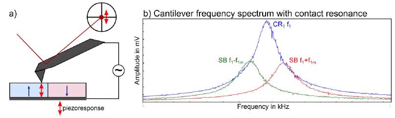
Figure 1: a) Schematic working principle of Piezoelectric Force Microscopy (PFM), where an AC voltage introduces a periodic sample oscillation, i.e., the piezoresponse, during a contact mode scan. The piezoresponse is detected via optical beam deflection using a superluminscent diode and a position sensitive photodetector. b) Amplitude of the contact resonance CR1 at frequency f1 in the frequency spectrum of the AC excitation with the two sidebands SB generated at f1±f1m used for the Dual Frequency Resonance Tracking (DFRT).
Experimental
For the DFRT PFM measurement on MAPbI3, we used a Park Systems NX10 coupled with a Zurich Instruments HF2 LIA. All measurements were conducted with a conductive full platinum 25Pt300B Cantilever from Rocky Mountain Nanotechnology, a nominal spring constant of 18 N/m and a vertical contact resonance in the range of 150-200 kHz. We chose a setpoint of ~160 nN. The scan rate was 0.25 Hz, the resolution 512×512 px and the scan size 10×10 μm².
Results and Discussion
The DFRT PFM measurements in Figure 2 were conducted on a large, isolated grain in a MAPbI3 thin film, prepared via solvent annealing to achieve large grain sizes and high crystallinity. The topography signal in this grain shows a predominantly flat and smooth surface with a root mean square roughness of ~1.5 nm. The out-of-plane PFM amplitude and phase revealed a distinct triangular domain structure located in the center of the grain, as well as some additional domain at the right edge of the grain. Upon further analysis via an averaged line profile, we found distinct amplitude minima at the sites of the domain walls and a 170° phase contrast, both indicative of an oppositely oriented ferroelectric polarization. However, due to the ion mobility and electronic properties of MAPbI3, which can impede on the PFM reliability, the ferroelectric character of the material has to be studied more in depth in the future.14
The DFRT frequency channel, which carries information on the local contact resonance and therefore contact mechanics between tip and sample, displays a distinct correlation with the PFM signals of phase and amplitude. As such, on the triangular domain the line profile shows a frequency shift of 20 kHz with respect to the bulk grain. In the absence of topography crosstalk due to the flat grain surface, the shift of the contact resonance suggests a change of the sample’s mechanical properties between the bulk and the domain. This change of the mechanical properties likely originates from the material’s ferroelastic character.7,15
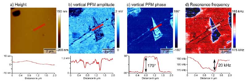
Figure 2: Vertical DFRT-PFM measurement on a large MAPbI3 perovskite grain in thin film. a) topography with flat smooth surface, b) PFM amplitude featuring the domain walls as amplitude minima, c) PFM phase with 170° phase contrast, indicating an opposite polarization orientation between bulk and domain, d) DFRT frequency carrying information on local contact resonance. The shift of the contact resonance by 20 kHz suggests nanomechanical differences between bulk and domain.
Conclusion
For this study, we successfully imaged a ferroelastic and possibly ferroelectric domain in a crystalline MAPbI3 grain via resonance enhanced Piezoelectric Force Microscopy (PFM) on a Park Systems NX10 Atomic Force Microscope (AFM) with a Zurich Instruments HF2 Lock In Amplifier. We showed that the additional frequency feedback in Dual Frequency Resonance Tracking (DFRT) not only stabilizes the PFM response with respect to topographic crosstalk, but also offers additional insights on local mechanical behavior via the DFRT frequency channel. Thereby, DFRT PFM allows the classification of the domain origin in MAPbI3 as ferroelastic with a possible ferroelectricity. The readily accessible measurement signals on AFMs from Park Systems facilitated a simple implementation and synchronization of the AFM and Zurich Instruments’ HF2 for DFRT PFM.
References
1. Poglitsch, A. & Weber, D. Dynamic disorder in methylammoniumtrihalogenoplumbates (II) observed by millimeterwave spectroscopy. J. Chem. Phys. 87, 6373–6378 (1987).
2. Kojima, A., Teshima, K., Shirai, Y. & Miyasaka, T. Organometal halide perovskites as visible-light sensitizers for photovoltaic cells. J. Am. Chem. Soc. 131, 6050–6051 (2009).
3. Stoumpos, C. C., Malliakas, C. D. & Kanatzidis, M. G. Semiconducting tin and lead iodide perovskites with organic cations: phase transitions, high mobilities, and near-infrared photoluminescent properties. Inorg. Chem. 52, 9019–9038 (2013).
4. Wilson, J. N., Frost, J. M., Wallace, S. K. & Walsh, A. Dielectric and ferroic properties of metal halide perovskites. APL Mater. 7, 10901 (2019).
5. Frost, J. M. et al. Atomistic origins of high-performance in hybrid halide perovskite solar cells. Nano Lett. 14, 2584–2590 (2014). 6. Röhm, H., Leonhard, T., Hoffmann, M. J. & Colsmann, A.
Ferroelectric domains in methylammonium lead iodide perovskite thin-films. Energy Environ. Sci. 10, 950–955 (2017).
7. Hermes, I. M. et al. Ferroelastic Fingerprints in Methylammonium Lead Iodide Perovskite. J. Phys. Chem. C 120, (2016).
8. Tagantsev, A. K., Cross, L. E. & Fousek, J. Domains in ferroic crystals and thin films. 13, (Springer, 2010).
9. Zubko, P., Catalan, G., Buckley, A., Welche, P. R. L. & Scott, J. F. Strain-gradient-induced polarization in SrTiO 3 single crystals. Phys. Rev. Lett. 99, 167601 (2007).
10. Warwick, A. R., Íñiguez, J., Haynes, P. D. & Bristowe, N. C. Firstprinciples study of ferroelastic twins in halide perovskites. J. Phys. Chem. Lett. 10, 1416–1421 (2019).
11. Soergel, E. Piezoresponse force microscopy (PFM). J. Phys. D Appl. Phys. 44, 464003 (2011).
12. Güthner, P. & Dransfeld, K. Local poling of ferroelectric polymers by scanning force microscopy. Appl. Phys. Lett. 61, 1137–1139 (1992).
13. Rodriguez, B. J., Callahan, C., Kalinin, S. V & Proksch, R. Dual-frequency resonance-tracking atomic force microscopy. Nanotechnology 18, 475504 (2007).
14. Liu, Y. et al. Dynamic behavior of CH3NH3PbI3 perovskite twin domains. Appl. Phys. Lett. 113, 72102 (2018).
15. Strelcov, E. et al. CH3NH3PbI3 perovskites: Ferroelasticity revealed. Sci. Adv. Adv. 3, e1602165 (2017).