


The 23nd Le forum des microscopies à sonde locale, the most important Atomic Force Microscopy meeting in France, will take place in the city of Saint-Valery on the Hauts-de-France coast on 2 - 5 November 2020. Park Systems is proud to announce its participation as an exhibitor!
Join us for THE LATE NIGHT AFM WORKSHOP:
"En explorant le potentiel du sideband KPFM" presented by Dr. Andrea Cerreta - Application Scientist Park Systems Europe, Mannheim, Germany
We will showcase the capabilities of the Park NX10, the High Resolution Research Atomic Force Microscope (AFM) with the wide range of nanomechanical, magnetic and electrical material characterization modes with a focus on new generation KPFM mode!
Le forum des microscopies à sonde locale
We will showcase the capabilities of the Park NX10, the High Resolution Research Atomic Force Microscope (AFM) with the wide range of nanomechanical, magnetic and electrical material characterization modes with a focus on new generation KPFM mode!
Register here: HERE
- Time: 2 – 5 November
- Venue: Cap Hornu Hotel and Restaurant, Saint-Valery-Sur-Somme
- Our location: Park Systems booth
Join our poster presentation:
"Better in Vacuum - how vacuum can improve investigation of 2D materials using conductive Atomic Force Microscopy (AFM)" presented by Dr. Romain Bourrellier - Sales Manager Park Systems France, Orsay, France
Le forum des microscopies à sonde locale
About Le Forum des Microscopies à Sondes Locales:
Started in northern France (Sangatte, 1998), the Forum travels around different French locations with a few stops at the Belgian neighbors..
The forum brings together each year about 150 researchers. It has become a landmark French meeting for the community of near-field microscopy.
The spirit of this forum has not changed since 1998; its goal is to bring together French-speaking (mainly France, Belgium, Switzerland) community of scanning probe microscopies (AFM, STM, SNOM and related techniques), from established researchers to students or industry representatives, to discuss the latest developments in the field. These advances concern basic studies in nanoscience as well as application and instrumentation. The relevance of this forum is growing with the years as the atomic force microscopy constitute one of the major tools of nanotechnologies. The technique allows, at the nanoscale, to study the physical and chemical properties (mechanical, electronic, optical, biological ...) of surfaces and nanosystems.
Link: http://www.sondeslocales.fr/forum2020
THE LATE-NIGHT AFM WORKSHOP, 2 November, 2020, 21.00 pm
Advances in Materials Nanocharacterization and Material Analysis
Exploring the Potential of the Sideband KPFM Mode
Andrea Cerreta1, Ilka Hermes1, Victor Bergmann1, Charles Kim2
1 Park Systems Europe, Mannheim, Germany
2 Park Systems Corp, Suwon, South Korea
Presenter: Andrea Cerreta, Park Systems Europe, Mannheim, Germany, acerreta@parksystems.com
Abstract
Kelvin Probe Force Microscopy (KPFM) is a scanning probe method that utilizes electrostatic forces between a nanoscopic, conductive tip and a sample for material characterization by mapping the distribution of the surface potential [1,2].
In the standard lift mode KPFM [3], the sample is first scanned in dynamic mode at close distance in order to retrieve its topography. During the second pass, the tip is retracted at a given lift distance and traces back the topography while electrically excited at the lever eigenmode frequency. Since the conductive tip is sensitive to the local gradient of the electrical field, one can minimize the amplitude or phase shift of the probe caused by such a gradient by applying a counteracting voltage on the tip, which would exactly compensate the sample potential at each pixel. This allows to detect and image the potential variation along each line of the scanned frame.
However, this dual-pass mode has several technical drawbacks. First, due to the lift height the electrical signal measured by the tip is necessarily an averaged contribution of a larger area of the sample during second pass, which implies a loss in lateral resolution. Second, since the tip needs to scan each line twice, a longer image acquisition time must be taken into account. On the other hand, a simultaneous mechanical and electrical excitation of the lever at its resonant frequency would cause a severe crosstalk between topographic and electrical signals.
In Park Systems tools, we are currently implementing the new sideband KPFM mode, which allows for simultaneous imaging of the topography and surface potential with a high spatial potential resolution and improved sensitivity with respect to lift mode and other KPFM (e.g. off-resonance) methods. Here, the topography is detected at the resonance of the cantilever, while the electrical drive of the KPFM is applied at much lower frequencies between 1 and 4 kHz. Due to frequency mixing, satellite peaks or sidebands appear in 1 and 4 kHz from the resonance. The parallel detection of both excitations is feasible due to the presence of multiple lock-ins in the Park NX default electronics. Since the KPFM signal is detected on the sidebands and the topography is detected on the resonance, both signals can be measured simultaneously.
The workshop will provide a theoretical introduction to KPFM and show live examples of sideband KPFM experiments using the Park NX20 Large Sample AFM.
Better in Vacuum - how vacuum can improve investigation of 2D materials using conductive Atomic Force Microscopy (AFM)
Jonathan Ludwig1,2, Marco Mascaro1,2, Umberto Celano1, Ilka M. Hermes,3,A Wilfried Vandervorst1,2, Kristof Paredis1, Andrea Cerreta3
1. IMEC, Leuven, Belgium
2. Department of Physics and Astronomy, University of Leuven, Leuven, Belgium
3. Park Systems Europe GmbH, Mannheim, Germany
A. Corresponding author: Ilka M. Hermes, ihermes@parksystems.com
In the last years, the aim of semiconductor industry to produce nanoscale-sized devices determined an increasing interest for a series of 2D materials [1]. Among them, transition metal dichalcogenides (TMDs) are under investigation due to some promising electrical characteristics, such as an inherent band gap and a relatively high mobility of charge carriers, exhibited at nanoscale on single grains or islands [2,3].
Atomic Force Microscopy (AFM) offers a platform for the simultaneous characterization of multiple properties of 2D materials. AFM allows to determine the structural conformation and growth of 2D materials and probe their local electrical response. We used AFM to perform this kind of correlative microscopy on MoS2 layers grown onto sapphire via Metal Organic Chemical Vapor Deposition (MO-CVD). The morphological and electrical properties of samples with different thickness were studied and compared by using Conductive AFM [4].
It is well known that water contamination strongly affects the properties of MoS2, because it leads to a p-doping of the material [5]. In order to assess the effect of water on the conductive properties of MoS2, AFM measurements were done both in air and in high vacuum using a Park HiVac AFM system. The vacuum allows to get rid of the water layer naturally present on the top of the sample in ambient conditions. Results showed a larger local conductivity in vacuum with respect to air. Moreover, conductivity maps in vacuum showed an increased sensitivity with respect to measurements in air, allowing to determine boundaries between different conductive grains.
The ability of AFM to resolve electrical properties at nanoscale and the current advancement of the AFM technology, which allows integrating these characterization tools into the semiconductor manufacturing process, make AFM the ideal platform for the study of these 2D semiconductor materials.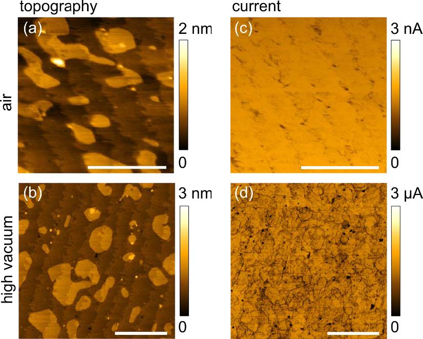
Figure 1: cAFM from the same 3-4 layered MoS2 sample showing the increased current level and sensitivity under high vacuum. (a) and (b) Topography (c) current images in air at 5 V bias (d) current images taken immediately after pumping to high vacuum at 0.5 V bias. The data taken in air and high vacuum was acquired using identical parameters: same probe with spring constant k of 7 N/m, set point of 10 nN, and 1 Hz scan rate. Scale bar is 500 nm.
Image courtesy: IMEC, Leuven, Belgium