


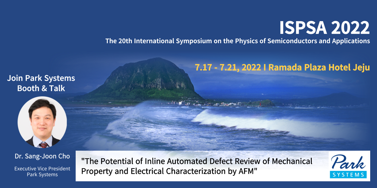
ISPSA 2022 will be held from July 17 to 21, 2022 with the theme of "Past-, Current-, and Future-Semiconductors" at the Ramada Plaza Hotel in Jeju.
Park Systems will participate in ISPSA 2022 to introduce excellent AFM technology and products, and specially, Invited Talk by Executive Director Dr. Cho is scheduled.
▶Date: July 18 - 21, 2022
▶Venue: Ramada Plaza Hotel, Jeju, Korea
▶Invited Talk: July 21, 11:30-12:00, "The Potential of Inline Automated Defect Review of Mechanical Property and Electrical Characterization by AFM" (by Dr. Sang-Joon Cho)
ABSTRACT
The Potential of Inline Automated Defect Review of Mechanical Property and Electrical Characterization by AFM
S.-J. Cho1*, S.-O. Km1, M. Lee1, Y.K. Lee1
1Application Technology Center, Park Systems Corp., Suwon, Korea
*Email: msjcho@parksystems.com
With decreasing device sizes, nanometer-sized defects on the wafer substrates can already limit the performance of the devices. The detection and precise classification of these defects requires additional characterization methods with a resolution in the nanometer-range. It is well known that AFM can measure not only surface morphology but also mechanical and electrical properties. However, the versatility of AFM is not fully utilized in industrial applications due to the various limitations. Various limitations include low throughput and tip life in addition to the laborious efforts for finding the defects in inline automated defect review (ADR). In this paper we introduce the ADR AFM with mechanical and electrical characterization capability of defects in addition to high throughput, high resolution, and non-destructive means for obtaining 3D information for nm-scale defect review and classification. This paper also introduces the potential application of the electrical characterization of ADR eventually leading to failure analysis. The advanced automated process and AFM-based physical property measurements enable ADR AFM to complement any manufacturing control toolset and easily accommodates wafer inspected by various inspection tools
This work was supported by National Grants of the Technology Innovation Program (20017507, Development of Metrology Inspection system for Semiconductor process based on Inline AFM and 20019223, Developing Automated Mask Repair Technology with EUV MASK Detec Detection and Analysis) funded By the Ministry of Trade, Industry & Energy (MOTIE, Korea) to S.-J. Cho.
References
[1] Zandiatashbar, A., Kim, B., Yoo, Y. K., Lee, K., Jo, A., Lee, J. S., Cho, S.-J., and Park, S. I., In Metrology, Inspection, and Process Control for Microlithography XXIX International Society for Optics and Photonics. March 2015, Vol. 9424, pp. 94241X.
[2] Zandiatashbar, A., Kim, B., Yoo, Y. K., Lee, K., Jo, A., Lee, J. S., Cho, S.-J., and Park, S. I., Photomask Technology 2015. International Society for Optics and Photonics, October 2015. pp. 96351A.
[3] Zandiatashbar, A., Taylor, P. A., Kim, B., Yoo, Y. K., Lee, K., Jo, A., Lee, J. S., Cho, S.-J., and Park, S. I, Metrology, Inspection, and Process Control for Microlithography XXX. International Society for Optics and Photonics, March 2016. pp. 97782P.
[4] Butt, Hans-Jürgen, Brunero Cappella, and Michael Kappl. Surface science reports 59.1-6 2005, pp1-152.
Link: https://www.ispsa.or.kr/