


Yanfeng Wang, Yanjun Yang, and Yiping Zhao Department of Physics and Astronomy, University of Georgia, Athens, GA 30602, USA
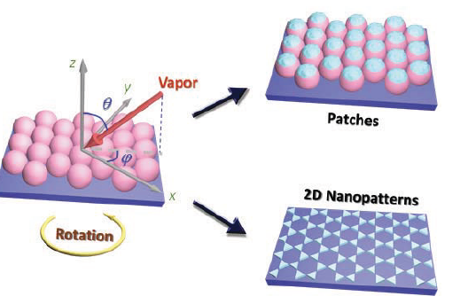
Figure 1. The general configuration of the nanosphere lithography and dynamic shadowing growth, and corresponding nanostructures that could be formed.
Introduction
Nanosphere lithography (NL) or natural lithography is a powerful but simple nanofabrication technique to produce arrays of nanostructures with hexagonal lattice arrangement.1-4 Such a method was first reported by Fischer and Zingsheimin 1981 when they used a close-packed microsphere monolayer as a shadow mask to fabricate platinum disks.5 When Van Duyne’s group introduced this method for nanostructure fabrication in 1995,2 it has then been widely investigated and evolved into one of the powerful nonconventional nanofabricationmethods.6-9 In general, the NL process uses a close-packed nanosphere monolayer (NSML) as a shadow/ etching mask, followed by multi-steps of deposition or etching or the combination of deposition and etching. Figure 1 illustrates the simplest situation for an NL process: a NSML is prepared on a flat substrate, and the substrate is used for vacuum deposition. Aft er deposition, two kinds of nanostructures are formed: the deposited material could form patches on top of the nanospheres or smaller structures would be deposited directly onto the substrates through the voids between the nanospheres (we called these structures twodimensional (2D) nanopatterns). The NSML could also be removed by different means so that only the 2D nanopatterns would be left on the substrates. Clearly, depending on the materials deposited or the final structures left on the substrates, the resulted nanostructures would have different physical or chemical properties. Since the nanospheres of various sizes can be purchased commercially,10 and vacuum deposition and plasma etching systems are readily accessible by many labs in the world, the NL method becomes a simple, aff ordable, and very popular nanofabrication technique. In addition, the NL process is also a versatile technique to design different and complicated nanostructure if the deposition configuration or the NSML could be modified. For the deposition configuration as shown in Figure 1, the vapor incident angle 0 (the angle between the vapor incident direction and the substrate surface normal) can be changed during the deposition so that the shadowing effect produced by the NSML could be varied. Also due to the periodicity and lattice symmetry of the hexagonal packed nanospheres, the deposition azimuthal angle φ (the angle between the projected vapor incident direction in x-y plane in Figure 1 with respect to one of the major axes of the hexagonal lattice (x-direction)) could also alter the shape of shadowing by the NSML. We broadly define the change of 0 and φ in deposition configuration as dynamic shadowing growth (DSG). For example, Van Duyne’s group has demonstrated the formation of elongated nanotriangle patterns by varying the 0 angle during the deposition.3 Kosiorek et al. has tuned both 0 and φ to design variety of nanostructures.11 In addition, by introducing etched NSMLs, complicated 2D nanopatterns can also be formed as demonstrated recently by Whitesides’s group.12 In fact, the change of the azimuthal angle φ would continuously produce different shapes of shadows, alter the location position and shape of the shadows; while the variation in the incident angle θ or the gap between the nanospheres could control the length and width of the shadows as well as their locations.
Here the versatility of the NL process by combining the NSMLs and DSG will be demonstrated. The morphologies of the resulting 2D nanostructures are characterized by an atomic force microscope (Park NX10) and their optical properties were obtained and related to the structural features.
Experiments
We use a home-made liquid-air interface method to assemble NSMLs as shown in Figure 2. In general, the creating of high quality NSMLs involved three steps, as shown in Figure 2a. The first step was to prepare well-dispersed nanosphere suspensions. The as-received polystyrene nanospheres were sonicated to ensure that they were well dispersed in liquid. Then the nanosphere suspension were “washed” several times by a centrifugation method. This washing procedure is necessary to remove surfactants that most companies put into the nanosphere suspension to stabilize the dispersion. The washing procedure was a critical step to improve the packing of the nanospheres during the formation of monolayers at the air-water interface. Then the suspension was dispersed/diluted in ethanol. The ethanol would help the nanospheres to quickly spread at the air-water interface. In Step 2, the cleaned nanosphere suspension was withdrawn into a syringe capped with a 20-gauge needle bent at a 90° angle towards a 15cm-diameter glass Petri dish partially filled with water. The Petri dish was carefully cleaned using a boiling piranha solution before used. The syringe was placed into a syringe pump and droplets of the nanosphere suspension were pumped into the water surface. When a droplet of the suspension landed onto the water surface, the ethanol lowered the local surface tension, causing the water to flow radially away from the dropping location, and carrying the nanospheres to spread on the surface quickly. As more and more nanospheres floated on the water surface and began to form a monolayer, the ethanol induced surface flow of water also acted as a compression mechanism to push the nanospheres to stay closer to each other so that the surface packing density of the monolayer could be significantly improved. Figure 2b shows a photo of the experimental set-up and Figure 2c is a photo of the Petri dish when a monolayer of nanosphere film was formed on the air-water interface. After a large area monolayer film was formed, a Teflon ring was placed around the perimeter of the Petri dish to prevent the nanospheres from depositing on the side wall of the glassware. Then more water was pumped into the Petri dish to raise water level so that desired pieces of substrates were carefully slid below the monolayer film. In Step 3, water was pumped out from the Petri dish, and as the water level was lowered, the monolayer would be deposited onto the substrates as the water level was lower enough. Then the substrates were dried for an extended time period. Figure 2d shows a representative SEM image of a high quality NSML made in our lab. Here polysterene nanospheres (Polysciences Inc.) with a diameter of D = 500 nm were used.
Once the NSMLs were formed on the substrates, the size of the nanospheres could be reduced by reaction ion etching through a Trion Technology Phantom III RIE/ICP system. The etching was conducted at 40 mTorr with a 10 sccm oxygen flow, an inductively coupled plasma power of 25 W, and a reactive ion etch power of 10 W for different etching time duration t = 0, 50, 75, 150, 200, 300, and 400 s, respectively. Different Ag nanostructures were then fabricated using a custom-built electron beam deposition system. The chamber was pumped down to a base pressure of < 1× 10⁻⁶ Torr. The deposition rate and total thickness of the films were monitored by a quartz crystal microbalance (QCM). Different NSML substrates etched at different time duration were loaded into the deposition chamber and Ag depositions were carried out at three different deposition configurations to show various simple 2D nanopatterns that could be formed: Strategy I: direct deposition of 60 nm (QCM thickness reading) Ag, i.e., 0 = 0o. It is expected that the nanopatterns formed are the projected void patterns of NSMLs. Strategy II: to set 0 = 53o and perform three consecutive depositions of 60 nm (QCM thickness reading) Ag at 0 = 0o, 120o, and 240o, respectively. The expected 2D nanopatterns should be three projected nanofeatures through the shadowing of the voids in NSMLs. Strategy III: to perform three consecutive depositions of 240 nm (QCM thickness reading) Ag at 0 = 10o and φ = 0o, 0 = 20o and 0 = 120o, and φ = 30o and φ = 240o, respectively. Since the projected shadow length is different at different 0 angle, the resulting nanopatterns should possess handedness property. Aft er the deposition, the samples were allowed to cool in vacuum before being removed from the chamber. Then the NSMLs were removed with the Scotch tape method. Any residual polysterene was washed away with toluene, and the samples were rinsed with acetone and then IPA before being dried under a N2 gas flow. The resulted nanostructures formed on the surface of the substrates from various NSMLs and deposition configurations described above, were predicted by an in-house ATLAB program.13 This program simulated the deposition process by projecting Ag vapor through the nanosphere monolayer mask at desired angles of θ and φ, but did not take into account of the shadowing effect of the thin film deposited on the PS nanospheres. Detailed information on this program can be found in Ref. 13. The morphologies of resulting samples were characterized by at atomic force microscope (Park NX10) and the corresponding optical properties were measured by a commercial UV−vis−NIR spectrophotometer (Jasco V-570) over a wavelength range of 400 nm to 2000 nm or by a home-built circular dichroism (CD) spectroscopic measurement system in a wavelength range of 400 nm to 1000 nm range.
Results and Discussion
Using AFM to characterize etched NSMLs
For the combined NSML and DSG method, it is very important to know the structure of the NSMLs, especially aft er plasma etching. Two methods could be used to characterize the etched NSMLs: direct imaging the etched monolayer or indirect measurement. For direct image method, one could take scanning electron micrographs (SEM) of the etched NSMLs and measure the size of the nanospheres as a function of the etching time. In most cases, the nanospheres we used are made by insulating materials,
such as polystyrene or silica. Also, since we concern the optical property of the resulting structures, the NSMLs are prepared on glass substrates or other insulating substrates. Therefore, it is very hard to use SEM to obtain clear NSML images due to heavy charging effect. The other conventional imaging technique is AFM. As shown in Figures 3a and 3b, representative D = 500 nm NSMLs before etching and aft er etching (t = 350 s) are shown. If one directly compares these two images by naked eyes, they do not show much diff erence as the etched gap for t = 350 s sample is not large enough, and also there is the AFM tip convolution effect that could smoothen the sharp changes in height near two adjacent nanospheres. In order to obtain the etching effect, the height profiles of the spheres through their apparent centers were obtained and plotted as a function of the scanned position as shown in Figure 3c. In order to minimize the effect of AFM tip effect, we intentionally removed several data points near the sharp changes between two adjacent nanosphere. The height data can be fitted by a circle function, as shown by the solid curves in Figure 3c. From the fitting, one can obtainthe effective diameter D of the etched nanospheres. Such a method requires very careful data analysis. The indirect method is to use the NSMLs as a shadow mask to directly deposit a layer of other materials at 0 = 0o (Strategy I). Aft er removing the NSMLs, one can use either the SEM or AFM to image the resulted structures, and one expects that inverted projected images of the NSMLs should be appeared. Here an unclaimed assumption was made, i.e., the resulting nanospheres still had a spherical shape, or the etching was isotropic. Figures 3d and 3e show the representative AFM images after the deposition of Ag by Strategy I for t = 200 and 400 s. We observe hexagonal patterned nanohole arrays with reduced nanohole diameter D when t increased. The hole diameter D was assumed to be the diameter of the etched nanospheres. Therefore, by plotting the D versus t, one could obtain the plasma etching performance for NSMLs (see Figure 3f). Based on our previous study,14 the diameter of the etched nanosphere should follow the relationship, D(t)=√(D2-(kt)2, where D0 is the initial diameter of the nanosphere while k is the etching rate. The red curve in Figure 3f shows the best fitting and we obtain k = 0.54± 0.02 nm/s.
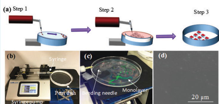
Figure 2 (a) Illustrations of the air-water interface method. (b) A photo of the home-made monolayer assembly system. (c) A photo showing nanosphere monolayer film floating on water surface in a glass Petri dish. (b) A representative SEM image of a high quality nanosphere monolayer on silicon substrate.
Morphology and optical properties of 2D nanopatterns by Strategy I
Figures 4a and 4b show the 2D patterns formed at small etching time for Strategy I, and the patterns formed for longer etching time are shown in Figures 3d and 3e. When the etching time t was small (Figure 4a), separated nanotriangle arrays in a hexagonal lattice were formed. When t increased to 150 s, adjacent nanotriangles started to connect together to form a 2D network (Figure 4b). When t increased further (t = 200 s, Figure 3d), a 2D nanohole network was formed, and the hole size became smaller when t increased to 400 s. Clearly, when t increased from 0 to 400s, the 2D patterns changed from discrete nanotriangle arrays to connected nanohole arrays, which are suggested from a shadowing deposition point of view since the gap between the nanospheres become larger when t increases. Thus, the optical properties of the 2D patterns are expected to have a transition from localized surface plasmon resonance (LSPR) to extraordinal optical transmission (surface plasmon propagation (SPP)).15 Figure 4c shows the UV-Vis transmission spectra of the 2D patterns formed at different etching time. For small etching time t (< 100 s), there was a main dip at λc = 954 nm which corresponds to a strong dipole resonance. This is consistent with other studies on nanosphere lithography and nanotriangle arrays.16-17 When t = 150 s and 200 s, the transmission spectra became very broad, and a dip could be extended beyond λ =1000 nm, which is due to the connection of nanotriangles shown in Figure 4b or Figure 3d. The connections redshifted the transmission dips. For t = 300 s and 400 s, a multi-dip and peak features were visible. Such a feature is due to a so-called extraordinary ptical transmission (EOT) effect discovered by Ebbesenet al. due to the nanohole network.18 The dip around λ = 650 nm is the Woods anomaly position while the broad transmission peak around λ = 700 nm is the EOT peak due to plasmon-grating coupling.19 Clearly, as the etching time increases, the morphology changes from disconnected nanotriangles to connected triangles, then to the nanohole network, and the optical response varies from LSPR to EOT.
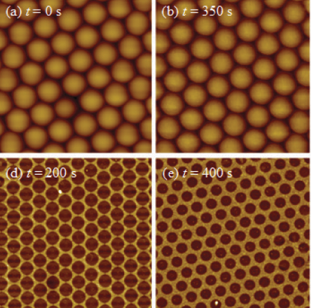
Figure 3 Representative AFM images of NSMLs for etching time t = (a) 0 s and (b) 350 s. The size of the images is 3 μm x 3 μm. (c) The height profiles of a single nanosphere before and aft er etching. The solid curves are the fitting results. Representative AFM images of Ag nanostructures deposited by Strategy I and aft er removing the nanospheres for t = (d) 200 s and (e) 300 s. The size of the images is 5 μm x 5 μm. (f) The plot of the hole diameter D from AFM images versus etching timet.
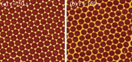
Figure 4Representative AFM images of 2D nanostructures for etching time t = (a) 50 s and (b) 150 s. The size of the images is 5 μm x 5 μm. (c) The UV-Vis transmission spectra of the samples deposited by Strategy I for various etching time t.
Morphology and optical properties of 2D nanopatterns by Strategy II
Figures 5a- 5c show some representative AFM images of the 2D patterns formed at etching time t = 200, 300, and 400 s for Strategy II. Since this strategy involves three different depositions, the patterns become more complicated but they can also be predicted by our in-house MATLAB program. The predicted structures are also shown in Figure 5. For t < 200 s, no 2D patterns were observed on the surface due to large vapor incident angle (0 = 53o) and small gaps between nanospheres. For t = 200 s, clusters of nanobars were formed (Figure 5a). Each cluster consisted of three nanobars, each bar had a 120o angle with respect to adjacent bars, which is consistent with the deposition strategy. In the MATLAB prediction, the lengths of the three bars were the same while from the AFM image, the lengths of the bars were 250±10 nm, 170±10nm, 170±10nm, and corresponding widths were 90±5nm, 99±4nm, and 98±5nm, respectively. The slight diff erence in the bar lengths was due to the extra shadowing effect induced by films deposited onto the nanosphere surfaces. For t = 300 s, two characteristic hole shapes could be formed according to the simulation: small triangular nanoholes and large irregular hexagonal holes (Figure 5b). The large hexagonal hole was the overlap of two large triangular holes with about 90o orientation diff erence. The AFM image shows almost the same pattern. Compared to Figure 5a, there were more Ag coverages in Figure 5b. For t = 400 s, also a complex hole pattern with two characteristic hole features was expected: one was a large triangle hole, and other was a windmill shaped hole (Figure 5b). The AFM image showed the exactly predicte features. In this case, the Ag had more coverage on the surface. For all the three samples measured by AFM, the thickness of the patterns were a constant, about 15 ±1nm.
The optical transmission spectra T(λ ) of the corresponding samples are shown in Figure 5d. For the t = 50 and 75 s samples, there was almost no spectral features resented in T(λ ) and the T(λ ) values of the entire wavelength range were close to 100%, which indicates that there were no nanostructures deposited on the substrate. However, for the t = 200 s sample, there was a sharp dip occurred at λc = 454 nm, which is the LSPR wavelength due to the nanobar clusters. For the t = 300 s sample, a larger dip occurred at λc = 460 nm; and for the t = 400 s sample, the resonance dip redshift ed to λc = 500 nm. Clearly when t increased, the dip value became smaller, which reflects a high absorbance. This is due to the factor that the Ag coverage on the surface became larger and larger with the increase of t.
Morphology and optical properties of 2D nanopatterns by Strategy III
Figures 6a - 6c show some representative AFM images of the 2D patterns formed at etching time t = 200, 300, and 400 s for Strategy III. Since this strategy involves three different depositions at different 0 angle, the shadowing length due to the nanospheres would be different in three azimuthal directions, which means the symmetry of the pattern would be broken, and the resulting structures should show certain handedness property, i.e., chirality. Figure 6a shows the patterns for t = 50 s sample, with disconnected double triangle clusters. For the t = 200 s sample (Figure 6b), larger connected triangular-shaped clusters were visible, and near each cluster, there was a small nanoparticle available. For t = 300 s sample (Figure 6c), honeycomb like networks were formed. Unlike the jointed triangular structures in Figure 4b or the nanohole networks shown in Figure 3d, the deposited Ag had an uneven distribution along the skeleton of the honeycombs. The joint of three adjacent arms (height ~ 145 nm) haa larger height than that (~ 80 nm) of the arms. Figure 6d shows the corresponding optical transmission spectra T(λ) of these samples. For the t = 50 sample, there was a transmission dip occurred at λc = 747 nm, which corresponded to the LSPR resonance of the disconnected double triangle features. When t increased to 100 s, the dip redshift ed to λc = 767 nm, which means the structures
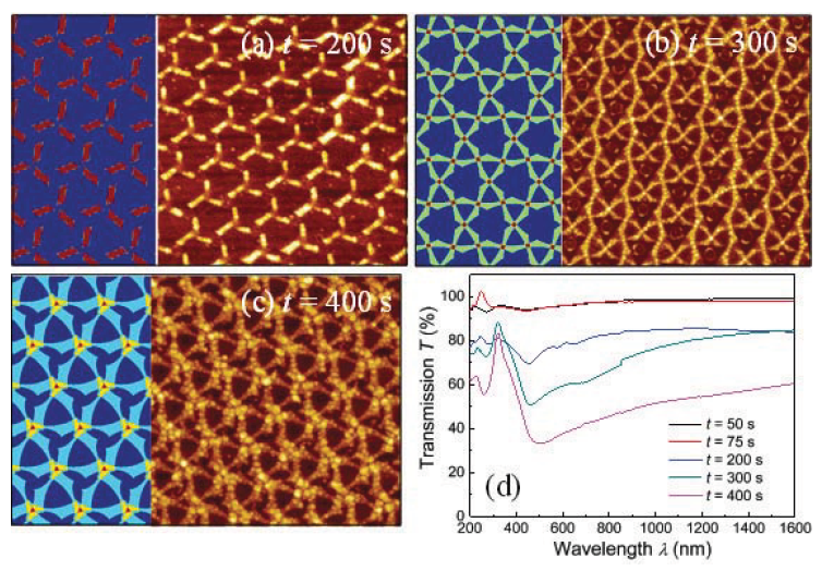
Figure 5 Representative AFM images of nanostructures deposited by Strategy II for etching time t = (a) 200 s, (b) 300 s, and (c) 400 s, respectively. The size of the images is 3 μm x 3 μm. The left panel of each AFM image shows the simulation result by our in-house MATLAB program. (d) The UV-Vis transmission spectra of the samples deposited by Strategy II for various etching time t.
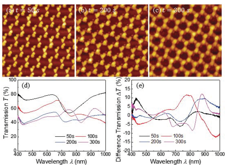
Figure 6 Representative AFM images of nanostructures deposited by Strategy III for etching time t = (a) 50 s, (b) 200 s, and (c) 300 s. The size of the images is 3 μm x 3 μm.
(d) The UV-Vis transmission and (e) The circular dichroism spectra of the samples deposited by Strategy III for various etching time t.
For the t = 200 s sample, the transmission over the entire spectrum became significant lower and there was a broad dip between λ = 650 to 850 nm. For the t = 300 s sample, an EOT type of response was obtained, with a dip at λ =832 nm and an EOT peak at λ = 926 nm. Since the resulted structures were expected to have handedness, which infers that when a right-hand or left -hand circularly polarized (RCP or LCP) light interacts with the structures, the response would be different. The difference between the transmission spectra of the LCP and RCP, ΔT(λ), called circular dichroism (CD) spectrum, should not be zero. Figure 6e shows the CD spectra of the corresponding samples. All the samples show non-zero CD spectra. For the t = 50 sample, a dip in ΔT(λ) occurred at λ = 732 nm, which is very close to the LSPR dip at λc = 747 nm. For the t = 100 s sample, a huge positive peak occurred at λ = 785 nm and a corresponding dip occurred at λ = 973 nm. For the t = 200 s sample, a broad peak appeared at λ = 877 nm. A sharp peak also was observed at the same location for the t = 300 s sample. Clearly all the samples demonstrated the CD response.
Conclusions
In summary, we have demonstrated that when combining NSMLs and DSG, various nanostructures can be designed and fabricated. The resulted nanostructures can be constructed by adjusting two sets of important parameters, the deposition configuration parameters, i.e., the vapor incident angle θ and the azimuthal angle φ; and the configuration of NSMLs, i.e., the gaps between the adjacent nanospheres. Also geometrically complicated nanopatterns could be designed by tuning the way to perform the deposition, for example, using multi-step deposition. AFM is a powerful technique to characterize the morphology of the resulting nanostructures and these nanostructures demonstrate different plasmonic properties and are expecting to have different applications.
Acknowledgments
This work is supported by the National Science Foundation under Grant ECCS- 1609815 and ECCS-1808271.
References
[1] Deckman, H.; Dunsmuir, J., Natural lithography. Applied Physics Letters 1982,41 (4), 377-379.
[2] Hulteen, J. C.; Van Duyne, R. P., Nanosphere Lithography - a Materials General Fabrication Process for Periodic Particle Array Surfaces. J Vac Sci Technol A 1995,13 (3), 1553-1558.
[3] Hulteen, J. C.; Treichel, D. A.; Smith, M. T.; Duval, M. L.; Jensen, T. R.; Van Duyne, R. P., Nanosphere lithography: Size-tunable silver nanoparticle and surface cluster arrays. Phys Chem B 1999,103 (19), 3854-3863.
[4] Zhang, G.; Wang, D. Y., Colloidal Lithography- The Art of Nanochemical Patterning. Chemistry-an Asian Journal 2009,4 (2), 236- 245.
[5] Fischer, U. C.; Zingsheim, H., Submicroscopic pattern replication with visible light. Journal of Vacuum Science and Technology 1981,19 (4), 881-885.
[6] Zhang, J. H.; Li, Y. F.; Zhang, X. M.; Yang, B., Colloidal Self-Assembly Meets Nanofabrication: From Two-Dimensional Colloidal Crystals to Nanostructure Arrays. Advanced Materials 2010,22 (38), 4249-4269.
[7] Li, Y.; Duan, G. T.; Liu, G. Q.; Cai, W. P., Physical processes-aided periodic micro/ nanostructured arrays by colloidal template technique: fabrication and applications. Chemical Society Reviews 2013,42 (8), 3614- 3627.
[8] Ye, X. Z.; Qi, L. M., Two-dimensionally patterned nanostructures based on monolayer colloidal crystals: Controllable fabrication, assembly, and applications. Nano Today 2011,6 (6), 608-631.
[9] Yang, S. K.; Lei, Y., Recent progress on surface pattern fabrications based on monolayer colloidal crystal templates and related applications. Nanoscale 2011,3 (7), 2768- 2782.
[10] Zhang, G.; Wang, D., Colloidal lithography— the art of nanochemical patterning. Chemistry–An Asian Journal 2009,4 (2), 236- 245.
[11] Kosiorek, A.; Kandulski, W.; Chudzinski, P.; Kempa, K.; Giersig, M., Shadow nanosphere lithography: Simulation and experiment. Nano Lett 2004,4 (7), 1359-1363.
[12] Nemiroski, A.; Gonidec, M.; Fox, J. M.; Jean- Remy, P.; Turnage, E.; Whitesides, G. M., Engineering Shadows to Fabricate Optical Metasurfaces. Acs Nano 2014,8 (11), 11061- 11070.
[13] Larsen, G. K.; He, Y.; Ingram, W.; Zhao, Y., Hidden chirality in superficially racemic patchy silver films. Nano Lett 2013,13 (12), 6228-32.
[14] INGRAM, W. THE FABRICATION AND APPLICATION OF PLASMONIC NANOPATTERNS BY SHADOW NANOSPHERE LITHOGRAPHY. The University of Georgia, Athens, GA, 2016.
[15] García de Abajo, F. J., Colloquium: Light scattering by particle and hole arrays. Reviews of Modern Physics 2007,79 (4), 1267-1290.
[16] Jensen, T. R.; Schatz, G. C.; Van Duyne, R. P., Nanosphere Lithography: Surface Plasmon Resonance Spectrum of a Periodic Array of Silver Nanoparticles by Ultraviolet−Visible Extinction Spectroscopy and Electrodynamic Modeling. The Journal of Physical Chemistry B 1999,103 (13), 2394-2401.
[17] Whitney, I.; Yizhuo, H.; Keenan, S.; William, M. D.; Dexian, Y.; Yiping, Z., Tuning the plasmonic properties of silver nanopatterns fabricated by shadow nanosphere lithography. Nanotechnology 2016,27 (38), 385301.
[18] Ebbesen, T. W.; Lezec, H. J.; Ghaemi, H. F.; Thio, T.; Wolff , P. A., Extraordinary optical transmission through sub-wavelength hole arrays. Nature 1998,391, 667.
[19] Li, Y., Plasmonic optics: theory and applications. SPIE Press: 2017.