


A Comparative Study of Atomic Force Microscopy between AM KPFM and Sideband KPFM, Principles and Applications
Research Application Technology Center, Park Systems Corporation
Introduction
Since the development of Atomic Force Microscopy (AFM) [1], several measurement modes have been developed to characterize electrical, mechanical, magnetic, and thermal properties. Among them, Kelvin Probe Force Microscopy (KPFM) [2] is a well-known mode that enables the monitoring of both surface morphology and surface potential distribution properties on a nanometer scale. KPFM has been utilized extensively to investigate the localized charge distributions on a surface layer [3], surface potential distributions [4] variations in surface work functions [5] and ferroelectric domains [6], in a variety of research fields. KPFM can simultaneously deliver both surface topographical information and surface potential/work functions of the sample by applying AC and DC voltage. Using the same configuration as Electrostatic Force Microscopy (EFM), KPFM monitors the surface potential and work function of samples by applying a DC bias (VDC) to nullify tip-sample potential difference. The VDC, controlled by the KPFM feedback, equals the surface potential (VS) and thereby generates the surface potential map.
In the conventional method, amplitude modulation (AM) KPFM, the measurement signal directly relates to the electrostatic force between sample surface and tip via the amplitude of the AC frequency signal (Figure 1a). This implies that AM KPFM is strongly affected by the whole AFM cantilever, which lowers the resolution and sensitivity due to an averaging effect [7] [8].
Sideband KPFM has an advantage in terms of the spatial resolution and sensitivity of the surface potential measurement compared to AM-KPFM [9]. The AC voltage (VAC) applied between AFM tip and sample, generates and oscillation in the electrostatic force and its gradient. This oscillation leads to a modulation of the resonance frequency of the cantilever (f0). In the frequency spectrum of the cantilever deflection, sidebands appear at f0 + fAC and f0 – fAC caused by the oscillating force gradient (Figure 1b). The application of a DC voltage, which matches the potential difference between the AFM tip and the sample, compensates for the electrostatic force and the sideband disappears. By measuring the DC voltage required to compensate for the electrostatic force, the surface potential distribution of the sample can be imaged, as well as the work function distribution, if the work function of the tip is known. Unlike AM-KPFM, the Sideband KPFM signal depends on the electrostatic force gradient and is therefore mainly affected by the AFM tip apex. The dependence on the force gradient leads to an improved spatial resolution and potential sensitivity.
In this study, we present results obtained with AM-KPFM and Sideband KPFM on well-defined samples with extended areas of different surface potentials. From these results, we directly compare the spatial resolution of AM-KPFM and Sideband KPFM under identical conditions.
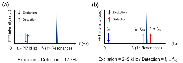
Figure 1. Frequency spectra for AM-KPFM (a) and Sideband KPFM (b).
Materials and Methods
Sideband KPFM
Sideband KPFM is an optional AFM mode used to measure electrical properties of a sample surface. Figure 2 shows the connection diagram of Sideband KPFM, which uses two lock-in amplifiers to measure the amplitude and phase of each sideband. On lock-in amplifiers 2 and 3, a signal with a frequency of f0 ± fAC is used as the reference signal (generated by lock-in amplifier 2) to decouple the sideband signals with a frequency of f0 ± fAC in the deflection signal (detected by lock-in amplifiers 2 and 3). The decoupled signals from the two lock-in amplifiers are averaged and used for the feedback to adjust the DC voltage. The AFM controller applies a corresponding VDC so the averaged sideband peak size becomes zero (as tip bias servo in Park SmartScan).
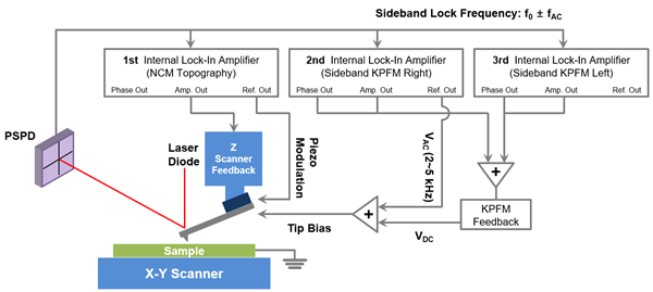
Figure 2. Connection diagram of Sideband KPFM..
Test samples and AFM cantilever
ZYH grade highly-ordered pyrolytic graphite (HOPG, SPI Supplies) was utilized for showing layer by layer surface potential differences. A silicone substrate with low conductivity polymer dots was used to display the surface potential contrast of two different materials. An IFX dopant calibration sample (NP20, Infineon) was chosen to monitor the stepwise electrical signal. This sample consisted of 5 different n-type implant areas in order to compare the electrical signals. All imaging was performed using an Au coated NSC36-C (resonance frequency, 65 kHz; spring constant, 0.6 N/m; length, 130 μm) with the same AFM parameters.
Results and discussion
This study analyzes three different samples to compare the electrical resolution performances of AM-KPFM and Sideband KPFM. Figure 3 shows surface potential images of HOPG by AM-KPFM and Sideband KPFM. Sideband KPFM confirms the sharp contrast due to the HOPG layer, whereas AM-KPFM shows blurry edges. As shown in the line profile analysis, Sideband KPFM has an approximately two-fold higher surface potential difference on layers (~70 mV) than AM-KPFM (~35 mV, red arrow). Also, Sideband KPFM displays small HOPG fragments very clearly, while AM-KPFM shows a blurry image.
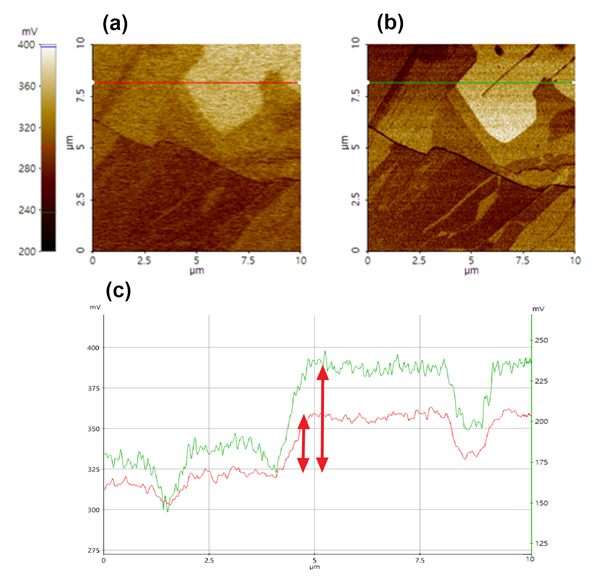
Figure 3. The comparison of surface potential between AM-KPFM (a) and Sideband KPFM (b) on a HOPG sample with a line profile analysis (c).
Next, the analysis of polymer dots on a silicone substrate was performed by AM-KPFM and Sideband KPFM. Additionally, Sideband KPFM both in and out of lift mode were compared to investigate the non-contact feedback performance for Sideband KPFM. In Figure 4, all images show contrasts between the polymer dots and the silicone substrate. However, AM-KPFM indicates a lower surface potential contrast than Sideband KPFM including lift mode. For Sideband KPFM, there is no significant difference between the no-lift mode and a 5 nm lift mode, which the line profile analysis confirms. Surface potential differences between the polymer dots and the silicone substrate are approximately 180 mV in AM-KPFM, ~300 mV for the no-lift Sideband KPFM, and ~330 mV for the 5 nm lift Sideband KPFM.
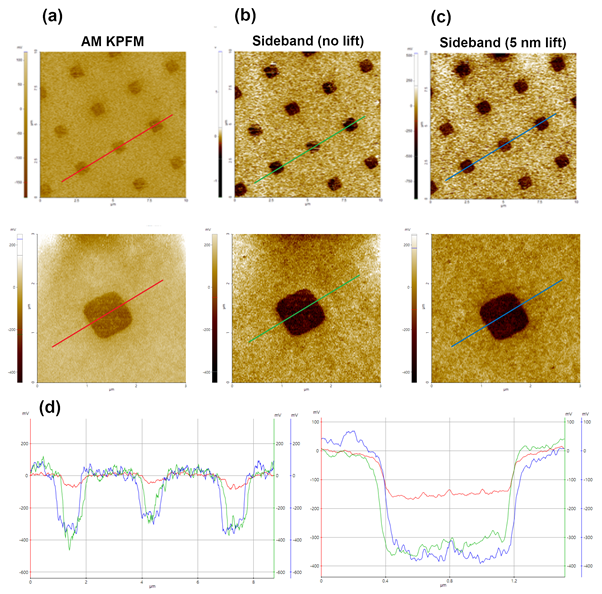
Figure 4. Comparison of surface potential between AM-KPFM (a), Sideband KPFM with no lift (b) and Sideband KPFM with 5 nm lift (c) on polymer dots sample with line profile analysis (d).
Lastly, AM-KPFM and Sideband KPFM were used on a IFX dopant calibration sample to compare stepwise electrical resolution. In AM-KPFM, different doping level of n-type implant are recognized; however, measurement of the steps in the electrical signal was difficult. In contrast, the stepwise electrical signal is displayed clearly in both no-lift and 5 nm lift Sideband KPFM. Based on several repetitive tests, all Sideband KPFM analyses show improved spatial resolution and potential sensitivity than those of AM-KPFM. As the line profile suggests, Sideband KPFM can monitor step-by-step surface potential differences, while AM-KPFM only detects a gradual signal decrease.
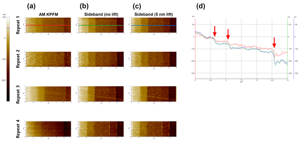
Figure 5. Multiple measurements on AM-KPFM (a), Sideband KPFM with no lift (b) and Sideband KPFM with 5 nm lift (c) on an IFX dopant calibration sample with line profile analysis (d).
Conclusions
In this study, we compare AM-KPFM and Sideband KPFM using a variety of samples. The results demonstrate that Sideband KPFM has superior spatial resolution and potential sensitivity compared to AM-KPFM. In surface potential images, Sideband KPFM shows a clear electrical contrast and detects relatively small potential changes. From line profile analysis, we find that the surface potential differences measured by Sideband KPFM are higher than that of AM-KPFM, underlining the superior performance of Sideband KPFM. Furthermore, the comparison between no lift and 5 nm lift in Sideband KPFM shows no difference for all tested samples. Due to the accuracy of Park Systems’s AFM feedback system, topography mapping is performed in True Non-Contact Mode without tapping between AFM tip and sample surface. Thus, it is possible to obtain the true surface morphology and a clear KPFM signal without crosstalk.
Since the development of KPFM, it has become one of the more useful AFM options utilized by surface material science and in semiconductor engineering. It is a unique technique for surface potential or work function mapping on the nanoscale, and the Sideband KPFM option offers superior spatial resolution and improved electrical sensitivity for material characterizations.
References
1. Quate, C. F., Gerber, C., & Binnig, C. (1986). Atomic force microscope. Phys. Rev. Lett, 56(9), 930-933.
2. Nonnenmacher, M., o’Boyle, M. P., & Wickramasinghe, H. K. (1991). Kelvin probe force microscopy. Applied physics letters, 58(25), 2921-2923.
3. Lü, J., Delamarche, E., Eng, L., Bennewitz, R., Meyer, E., & Güntherodt, H. J. (1999). Kelvin probe force microscopy on surfaces: investigation of the surface potential of self-assembled monolayers on gold. Langmuir, 15(23), 8184-8188.
4. Liu, L., & Li, G. (2010). Electrical characterization of single-walled carbon nanotubes in organic solar cells by Kelvin probe force microscopy. Applied Physics Letters, 96(8), 33.
5. Bieletzki, M., Hynninen, T., Soini, T. M., Pivetta, M., Henry, C. R., Foster, A. S., ... & Heiz, U. (2010). Topography and work function measurements of thin MgO (001) films on Ag (001) by nc-AFM and KPFM. Physical Chemistry Chemical Physics, 12(13), 3203-3209.
6. Wu, W., Horibe, Y., Lee, N., Cheong, S. W., & Guest, J. R. (2012). Conduction of topologically protected charged ferroelectric domain walls. Physical review letters, 108(7), 077203.
7. Melitz, W., Shen, J., Kummel, A. C., & Lee, S. (2011). Kelvin probe force microscopy and its application. Surface science reports, 66(1), 1-27.
8. Garrett, J. L., & Munday, J. N. (2016). Fast, high-resolution surface potential measurements in air with heterodyne Kelvin probe force microscopy. Nanotechnology, 27(24), 245705.
9. Stan, G. (2020). High-speed digitization of the amplitude and frequency in open-loop sideband frequency-modulation Kelvin probe force microscopy. Nanotechnology.