


By Hubert H. Cho
As a high school student interested in physics, I was fortunate to participate in an internship at Park Systems, which is a nanotechnology company that develops and produces atomic force microscopes (AFM). The AFM is one of the most widely used scientific instruments within the scanning probe microscopy (SPM) family and I was really excited because the SPM inventors won the Nobel Prize in Physics (1986) just four years after its invention [1]. The internship experience was perfect for me and it was a fantastic opportunity to see what life is like in a quickly growing company like Park Systems that has become a global leader in its field.
During my internship, I started off by helping to translate 300 pages of a user manual from English to Korean. The manual contained many terms related to engineering, physics, and mathematics so it was challenging but rewarding and I felt like I was taking advanced engineering classes for a semester. It was a crash course into a cutting-edge topic that opened my eyes.
During this time, I learned a lot about how nanoscience has been expanding into the development of analytical instruments, which is the next frontier of tools used in civilization and enabling advances in fields like semiconductors. The AFM is considered a third-generation microscope and allows humans to see what electron microscopes and optical microscopes cannot. People say that is why the AFM is considered the key to opening the world of nanotechnology. The AFM can function in a variety of capacities, like a Swiss Army knife, and not only allows you to observe the nanoworld, but to also explore and gather information. Because the AFM uses customizable probes to investigate nanoscale surface features, it can not only detect physical, electrical, and magnetic properties, but can also transform and manipulate chemical samples on a surface. Just like how over 20 Nobel Prizes were awarded for discoveries made using particle accelerators, remarkable discoveries about nanoworld phenomena are expected to occur from future AFM research.
During my time as an intern at Park Systems, I also learned that the company CEO, Dr. Sang-il Park, participated in the development of SPM technology in the laboratory where the world's first AFM was invented. This experience occurred during Dr. Park’s Ph.D. studies in Physics at Stanford University and led him to start the world's first company to commercialize the AFM in Silicon Valley. Even as Park Systems grows into one of the world’s leading instrumentation companies, I could still feel a strong entrepreneurial energy and pride at the company and imagined what it must have been like for Dr. Park to pioneer AFM commercialization from the heartland of innovation.
Once I finished translating the manual and acquiring background AFM knowledge, I felt ready for the big leagues and got an opportunity to learn about the Park Systems FX40 model, which is the world's most advanced AFM and has artificial intelligence functions along with various other automation features. The FX40 was just released in mid-summer and taught me about how scientific instrumentation should be not only powerful but also user friendly.
While AFM has many functions, it has traditionally been difficult to operate so it is typically used only for cutting-edge research by seasoned experts. Amazingly, after just a day of training with the advanced FX40 model that emphasizes an easy user experience, I was able to operate it by myself and successfully took AFM images. I even engraved my school logo and my name in a sample at the nanometer scale.
These activities piqued my curiosity and led me to conceive a personally satisfying experiment to compare my hair fibers with those of my dog. In a recent paper published in the journal Forensic Science International, 42 types of dog hairs were compared by optical microscopy and hair fiber analysis can be useful as supporting evidence in court trials [2]. As seen in that paper and in my own experiences, it can be quite difficult to distinguish the properties of individual hair fibers by using optical microscopy. However, morphological differences between my hair fibers and those of my dog could be readily seen by using the AFM (Figure 1). I have great hopes that the AFM may also be used eventually to support forensic investigations like how polymerase chain reaction (PCR) testing has been used for forensic profiling.
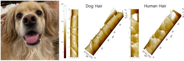
Figure 1. Differences in the height, shape, and roughness of hair fibers can be clearly seen by comparing 3D images of dog and human hair fibers by AFM measurements.
A while back, I had seen a remarkable picture in a newspaper article that told the story of the world's smallest Hebrew Bible, which had been etched onto a microchip using nanolithography (Figure 2).
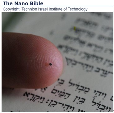
Figure 2. The world’s smallest copy of the Hebrew Bible is a gold-plated silicon chip that is the size of a pinhead and is engraved with the text of the entire Hebrew Bible. The text consists of over 1.2 million letters and was carved on the 0.5mm² chip by using a focused ion beam.
During my internship, I was able to experience a similarly amazing process with the AFM technique, which can also perform nanolithography. To do so, the AFM uses a high probe loading force to mechanically scratch the surface, or an electrical bias between the probe tip and surface can be applied to oxidize the surface. While the local oxidation method is widely used in nanoscale conducting and semiconducting surface patterning techniques [3,4], I decided to learn about a recently developed ferroelectric domain switching lithography technique. It patterns local domains of a PZT (lead zirconium titanate) film on a silicon wafer [5].
Patterns produced by ferroelectric domain switching can be read by Piezoelectric Force Microscopy (PFM), which is an advanced AFM mode that is useful for various applications involving actuators, sensors, and capacitors [6]. In a nutshell, PFM is sensitive to the ferroelectric domain's amplitude and phase (quadrature) values and can read this information to generate a PFM Quad image.
Inspired by the Hebrew Bible engraving example, I designed a bitmap image that depicted my school name and personal name and wanted to see if I could pattern them on a surface using the ferroelectric domain switching lithography method [7]. Figure 3 shows the overall bitmap design pattern and resulting 2D and 3D PFM Quad images along with conventional height-mode AFM images that were all recorded after the lithography process was completed.
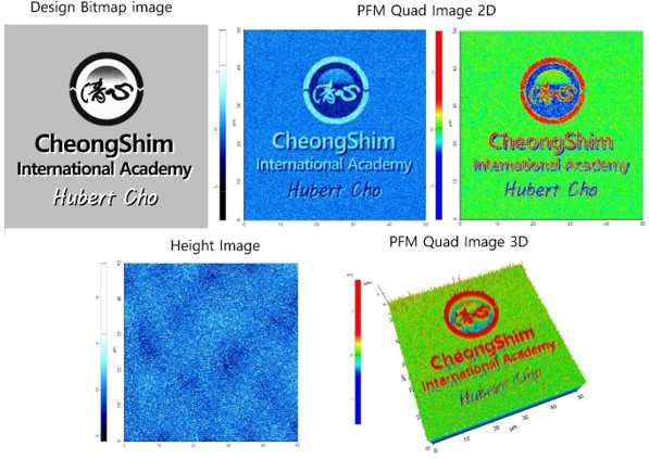
Figure 3. Bitmap image and ferroelectric domain switching lithography to create a nanoscale engraved pattern.
As shown in Figure 3, the AFM height image showed a flat surface without discernable pattern. In remarkable contrast, the PFM quad images matched the bitmap design, illustrating successful patterning and ferroelectric domain switching. This experience was remarkable and led me to read about other advanced functions, such as Magnetic Force Microscopy (MFM), that can be used to observe the magnetic recording signal of hard disks. I hope that I will get a chance to do another internship in the future but, for now, I am just thankful that Park Systems gave me the opportunity to see the nanoworld up close and firsthand.
It was a great experience to complete my internship at Park Systems and to learn about the cutting-edge FX40 AFM technology. I am very thankful for this wonderful experience and appreciate all the team members at Park Systems. I look forward to embarking on the next stage of my academic studies and will always cherish the memories of my internship.
References
[1] Binnig, G. et al.: Atomic force microscope. Physical Review Letters, 56 (9) 930 (1986)
[2] Vaishnav, Lakshika, et al. "A study on hair analysis of different Canidae breeds." Forensic Science International: Reports 3 100169 (2021)
[3] Minne, S. C. et al.: Atomic force microscope lithography using amorphous silicon as a resist and advances in parallel operation. Journal of Vacuum Science & Technology B: Microelectronics and Nanometer Structures Processing, Measurement, and Phenomena, 13 (3) 1380-1385 (1995)
[4] Garcia, R. et al.: Nano-chemistry and scanning probe nanolithographies. Chemical Society Reviews, 35 (1), 29-38 (2006)
[5] Li, D. and Bonnell, D. A.: Ferroelectric lithography. Ceramics International, 34 (1) 157-164 (2008)
[6] Soergel E. Piezoresponse force microscopy (PFM). Journal of Physics D: Applied Physics. 44(46):464003 (2011)
[7] Advanced Vector Nanolithography Using Closed Loop Scan System (2010, Online Article). Retrieved from: https://parksystems.com/park-spm-modes/97-mechanical-properties/251-nanolithograpy