


Monday, 04 Oct, 2021
- 11:00 AM
(ARAB)
Riyadh - 1:30 PM
(IST)
New Delhi - 4:00 PM
(SST)
Singapore - 6:00 PM
(AEDT)
Sydney
Since atomic force microscopy (AFM) is developed, various applications of nanotechnology were established, and those applications have led technological advances in many science fields. Researchers can acquire detailed topography of nanostructure and accurate probe positioning and distance control in nanometer resolution. Based on those benefits from AFM’s practical imaging capability, various applications were developed and enabled many innovative material property characterizations. However, those technological advances by nanotechnology have limited in ambient environment. Very soft samples like biological samples in liquid environment, there is not much successful advances with high impact. Because of unexpected physical contact of AFM tip on sample surface, small and fragile structures can be dragged or scratched. To overcome these limitation, Scanning ion conductance microscopy (SICM) was invented. The SICM uses nano pipette with ~100 nm inner diameter as a probe and the fundamental operation of SICM relies on an ion current that flows between a pipette electrode and a bath electrode. This ion current is used as feedback signal to maintain a constant distance between the nano pipette and the sample, allowing the nano pipette to scan the surface for topography imaging with non-contact. The SICM has the advantage of being able to cover applications that are difficult to apply AFM, so it is being used in various fields such as biology, electrochemistry, material science and battery research.
Presented By :
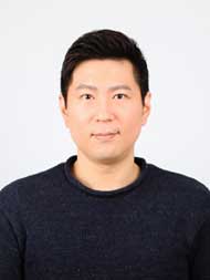
Dr. Jake Kim, Park Systems Korea
Dr. Kim received Ph.D. degree in Materials Science and Engineering from Nanyang Technological University, Singapore. He joined Tokyo Institute of Technology International Research Opportunities Program (TiROP) in 2014 and was engaged in nano-scale chemical composition analysis using scanning probe microscopy (SPM). From December 2017, he started to work in Park Systems as the manager of application technology center. He is specialized in the enhancement of nano-machanical measurement performance for Atomic Force Microscopy (AFM), building up a accurate and reliable environment for electrochemical measurement using Scanning Probe Microscopy (SPM; SECM,SECCM) and Scanning Ion Conductance Microscopy (SICM) applications development for biology.