


Enriching your AFM data: KPFM high resolution imaging of ferroelectric domains with automated AFM
Wednesday, 16 February 2022
-
10:00 am – 11:00 am
(GMT)
London, Dublin -
11:00 am – 12:00 pm
(CET)
Berlin, Paris, Rome -
19:00 pm – 20:00 pm
(UTC+9)
Seoul, Tokyo
Check out all webinars from the Empowering AFM Imaging series
here.
The formation of layered materials heterostructures affords a unique
degree of freedom in material design: the inter-layer twist angle. By
modifying the twist angle between two crystalline materials, the
registry of atoms may be continuously modified on length scales on the
order of 0.1 to 1000 nm, supporting a host of exotic phenomena such as
Wigner crystals [1], flat bands [2] and superconductivity [3]. Among
all state-of-the-art characterisation techniques, scanning probe
microscopy is particularly powerful tool in the study of such samples
since it can be used to measure both atomic registry of such layered
materials heterostructures and their associated functional properties
at sub-nanometre length scales. One such property to have received
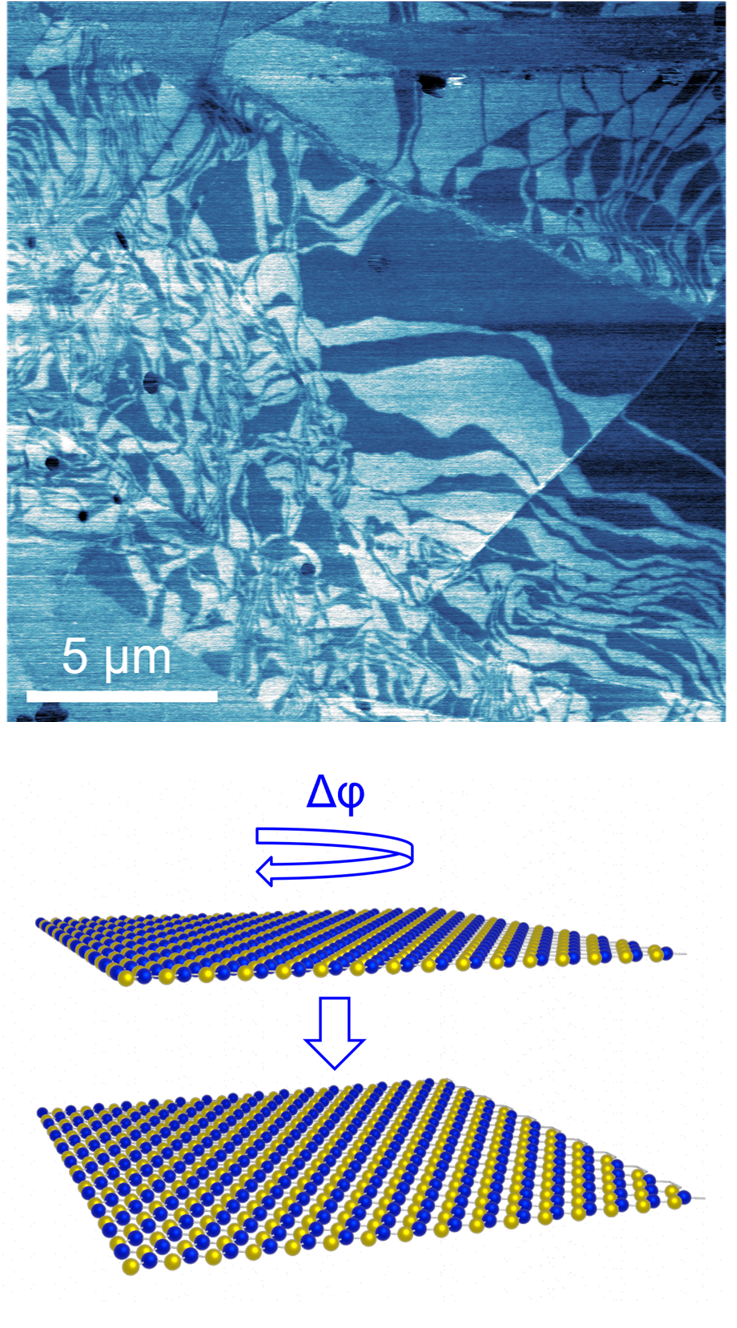
extensive recent attention is the formation of ferroelectric domains
in parallel stacked hBN [4-6]. In this webinar, we discuss the
characterisation of ferroelectric bilayer hBN using scanning probe
microscopy on the Park FX40 Automatic AFM.
In the first part of the demo, an overview of formation of
ferroelectric hBN samples and the operating principles of Kelvin
probe force microscopy (KPFM) will be given. We will then provide a
whistle-stop tour of the factors limiting the resolution and
accuracy of contact potential difference (CPD) measurements in KPFM,
and how these are better minimised using sideband KPFM. In the
second part of this webinar, a live demonstration of KPFM carried
out on ferroelectric bilayer-hBN on the Park FX40 system will take
place. We will first exhibit the unique automation available on the
Park FX40 system, enabling rapid preparation of AFM experiments. We
will then proceed to discuss the setup of both electrostatic force
microscopy (EFM) and frequency modulated sideband KPFM in order to
map the work function of layered materials and ferroelectric domains
in twisted bilayer hBN.
In addition to
showcasing the unique automation in both the setup and execution of
AFM experiments provided by the new FX40 AFM, we demonstrate a
workflow to characterise the morphology and strength of
ferroelectric domains in layered materials with state-of-the-art
spatial resolution and electrical sensitivity.
This work will be taken forward in further webinars where we address
electron tunnelling from graphene through ferroelectric hBN on the
nanometre scale which can be used to deterministically switch domains
and induce asymmetry in point current-voltage characteristics of such
samples, with applications both to memristive devices and tunnel
diodes capable of offering increased logic per chip.
[1] H. Li et al. Nature 597, 650–654 (2021).
[2] E. Li et al. Nat Commun 12, 5601 (2021).
[3] Y. Cao et
al. Nature 556, 43–50 (2018).
[4] C. R. Woods et al. Nat Commun.
12, 347 (2021).
[5] K. Yasuda et al. Science 372, 6549 1458
(2021)
[6] M. Vizner Stern et al. Science 372, 6549, 1462,
(2021).

Presenter:
Dr. James Kerfoot, Application Scientist at Park Systems United
Kingdom
James received his PhD in Physics from the University of Nottingham in 2018, studying the morphology and optical properties of monolayers of self-assembled molecules and their heterostructures. He then went on to work as a postdoctoral researcher, also at the University of Nottingham, working on the formation of hybrid heterostructures of molecular assemblies and layered materials demonstrating both electroluminescence and selective triplet excitation. In 2020, James took up a position as a postdoctoral researcher at the Cambridge Graphene Centre, using scanning probe microscopy and optical spectroscopy to study electrostatics and optical properties of layered materials heterostructures with controlled twist angle and their scalable incorporation into integrated photonic circuits. Since January 2022, James has been a member of the Park Systems team as an applications scientist, supporting customers with interest ranging from fundamental physics to industrial scale production in the application of a diverse range of scanning probe microscopy techniques to gain insightful results.