


Nanoscale Material Patterning using Atomic Force MicroscopyNano-Lithography
John Paul Pineda, Charles Kim, Cathy Lee, Byong Kim, and Keibock Lee
Park Systems Inc., Santa Clara, CA USA
INTRODUCTION
Nanotechnology has received increased attention within the scientific community due to its application in a number of fields ranging from electronics to biomedical technologies [1]. Progress in many of these applications depends mainly on the capability to fabricate nanostructured materials that include polymers and semiconductors, among others [2, 3]. Several methods have been introduced for the fabrication of nanostructures; the more common ones are electron beam lithography and focused ion beam lithography. However, these methods are not straightforward and are expensive to operate. One powerful method designed to overcome these problems is atomic force microscopy (AFM) nanolithography [1-3]. This technique is simple and less expensive [2]. AFM nanolithography is divided into two general groups based on their mechanistic and operational principles, bias-assisted and force-assisted AFM lithography [2]. In bias-assisted method, a bias voltage is applied to the tip to generate an oxide pattern on metallic or semiconductor substrate [4, 5]. Whereas, force-assisted method applies a large force to the tip to produce fine grooves on the surface of polymer like samples by mechanically scratching, pushing or pulling the surface atoms and molecules with a sharp tip; the interaction between the tip and the sample is mainly mechanical [2, 3].
In this technical note, we demonstrate the capability of AFM nanolithography to generate nanopatterns by utilizing Park NX10 Atomic Force Microscope. The tip bias mode is used to create oxide patterns on the silicon substrate. Successful pattern fabrication is confirmed by Lateral Force Microscopy (LFM). The integration of lithography and LFM mode with AFM enables it to fabricate nanopatterns and simultaneously acquire both topography and frictional data. The results obtained in this experiment confirms the fabricated oxide nanopatterns are successfully executed.
Experimental
A Park NX10 AFM was used for AFM nanolithography to draw nanopatterns onto a silicon substrate. LFM imaging was conducted after the lithography process to confirm the successful fabrication of the oxide patterns on the surface as well as to distinguish the surface difference between the oxide layers and silicon substrate. A PPP-CONTSCPt cantilever with a nominal spring constant (k = 0.2 N/m) and resonance frequency (f = 25 kHz) was utilized in the experiment.
Results and Discussion
Bias-Assisted AFM Nanolithography
Bias-Assisted AFM Nanolithography is a technique described as material modification (oxidation) through the application of voltage bias to the AFM tip. The applied bias on the tip results in the generation of an electric field between the tip and the sample. The field ionizes water molecules formed between the tip and the sample, which leads to local anodic oxidation (LAO) used to fabricate nanoscale oxide features on the surface. In the lithography process, the tip acts a nanoscale electrode for current injection or collection [1, 2]. The amount of oxide layer formed on the surface depends on the magnitude of the applied bias and humidity. Previous study [2] reported that the thickness of a pre-designed nanoscale oxide pattern of device structure increased due to the increment of applied tip voltages. Therefore, it concluded the tip voltage influenced the amount of oxide formed in the surface. Figure 1 shows a schematic illustration of bias-assisted AFM nanolithography. In this study, Park lithography software was used to design and apply nanolithography to the sample surface. A silicon substrate was used as a sample. The application of –10 V resulted in a high electric field around the tip which led to cleavage of water molecules into ions H+, OH- and O- ions [5]. The OH- and O- ions are then pushed away from the biased tip and react with silicon to form SiO2. The nanoscale oxide pattern forms on the surface of the silicon substrate along the scan area of the lithography scan.
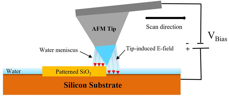
Figure 1. Schematic illustration of Bias-Assisted AFM Nanolithography [4, 5].
Lateral Force Microscopy
In Lateral Force Microscopy (LFM) mode, the vertical deflection and the torsion of the cantilever are measured and utilized to acquire topography and surface frictional characteristics of the sample. The cantilever movement in both the vertical direction and the torsion is tracked via a position sensitive photo detector (PSPD) that consists of four domains (a quad-cell), shown in Figure 2. Surface topographical information and frictional information are obtained using Equation 1 and 2.
Equation 1: Topographic information = (A+C) - (B+D)
Equation 2: Frictional information = (A+B) - (C+D)
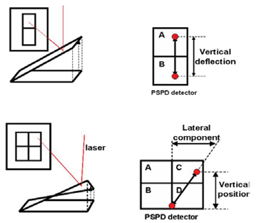
Figure 2. Schematic illustration of laser position on PSPD in the operation of AFM (top) and LFM (bottom).
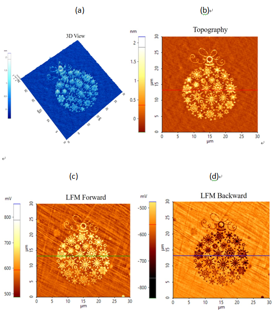
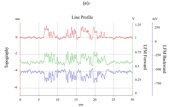
Figure 3 shows the topography, frictional data and equivalent line profile of the images after the lithography process. The images were taken using LFM mode. Since LFM is a contact mode, both topography and frictional data can be acquired simultaneously, allowing for correlation between topographic and frictional properties. The AFM topography image (Figure 3b) reveals that the design is a Christmas ball pattern with diameter of approximately 17 µm and composed of multiple tiny structures with heights ranging from 0.2–1.5 nm. Figure 3e represents the line profiles that were generated using the Park XEI software to provide a more direct signal comparison. By analyzing the line profiles obtained from the LFM forward (green line) and backward (blue line) scans, we gain insight into the frictional characteristics of the sample. In the forward scan, the LFM signal shifted upward, indicating that the movement of the cantilever was hindered due to change in frictional force as the tip bypassed the oxide layer. Conversely, the LFM signal shifted downward during the backward scan, which, again, was a result of the cantilever being dragged by the surface because of the larger frictional interaction between the cantilever and the surface. As a result, we can conclude that the frictional coefficient of the oxide layer is higher than that of the silicon substrate.
Conclusion
Here we have demonstrated the use of AFM nanolithography to generate nanoscale oxide patterns in a silicon substrate using the Park NX10 system. Voltage bias-mode technique was used in the AFM nanolithography process. The application of –10 V voltage bias on the tip led to successful fabrication of the nanoscale oxide features in the surface. LFM mode was also conducted and the results confirmed the successful fabrication of the oxide patterns. Overall, the AFM nanolithography described in this study is an effective method to fabricate next generation materials and devices with nanoscale features.
REFERENCES
1. A. Pimpin, et al., Review on Micro- and Nanolithography Techniques and their Applications.Enginering Journal.
2. S. Hutagalung, et al., Nanoscale Patterning by AFM Lithography and its Application on the Fabrication of Silicon Nanowire Devices. Sains Malaysiana 43(2), (2014): 267–272.
3. R. Garcia, et al., Advanced scanning probe lithography. Nature Nanotechnology 9, 577–587 (2014); doi:10.1038/nnano.2014.157
4. J. Voves, Nanoelectronics and nanolithography. https://www.researchgate.net/publication/228859246_Nanoelectronics_and_nanolithography
5. A. Bernal et al., LOCAL ANODIC OXIDATION ON SILICON (100) SUBSTRATES USING ATOMIC FORCE MICROSCOPY. http://www.scielo.org.co/pdf/dyna/v79n174/v79n174a08.pdf