


Chao Wen
Ms. Chao Wen received her B.S. (2018) in Physics from the Wuhan University of Technology and her first M.S. in Nanoscience from the Rovira i Virgili University. She obtained the International Exchange and Overseas Training Scholarship from Soochow University during her stay in Spain to study the current generation in ZnO nanowire arrays using conductive atomic force microscope (CAFM). Ms. Chao Wen is now pursuing her second M.S. in Physics at Soochow University with an expected graduation date of June 2021. During her master in Soochow University, Ms. Chao Wen received several awards, including the Excellent Master Student Award, the Principle Scholarships, and the National Scholarship. Her research focuses on the characterization of nanoelectronic behaviors across dielectrics using CAFM and two-dimensional materials-based resistive switching devices. She has published 8 research articles in top journals (including Nature Electronics, Advanced Materials, Advanced Functional Materials, etc.) and 3 conference proceedings. Ms. Chao Wen also serves as a technical reviewer for Scientific Reports and Microelectronic Engineering.
1. Please summarize the research you do and explain why it is significant?
My current research focuses on the characterization of nanoelectronic behaviors across dielectrics which are compatible with two dimensional (2D) materials using conductive atomic force microscope (CAFM). In order to solve the problem of limited switching speed in silicon-based microelectronic devices, 2D materials, such as graphene and transition metal dichalcogenides (TMDs), have been introduced into microelectronic devices due to their high carrier mobility. However, the interface between these 2D materials and 3D traditional dielectrics (such as SiO2 and transition metal oxides) is always problematic for the reason that there are plenty of dangling bonds on the surface of solid dielectrics. The problematic interface containing abundant defective bonds will impair the performance of microelectronic devices. Therefore, finding ultra-thin dielectric materials compatible with graphene and related materials is of utmost importance.
2. How might your research be used?
In my work, I aim to find ultra-thin dielectrics which are compatible with 2D materials. To realize this goal, I analyze the microstructure and nanoscale electrical properties (uniformity, point-to-point variability and dielectric strength) of these dielectrics. The nanoscale electrical and morphological analysis obtained from my research can not only help to reveal the reason for the electrical performance of microelectronic devices but also provide substantial information for other researchers to choose the proper dielectric for their devices. For example, my paper published in Advanced Materials proves that ultra-thin CaF2 films grown by molecular beam epitaxy show ultra-low variability, high dielectric strength, and low leakage current. This means that the use of ultra-thin CaF2 films may be one possible solution to the problematic interface between 2D materials and traditional solid dielectrics. This can further solve the challenging problem for the integration of 2D materials into Si based microelectronic devices. This is what I hope to bring to the electron devices society as well.
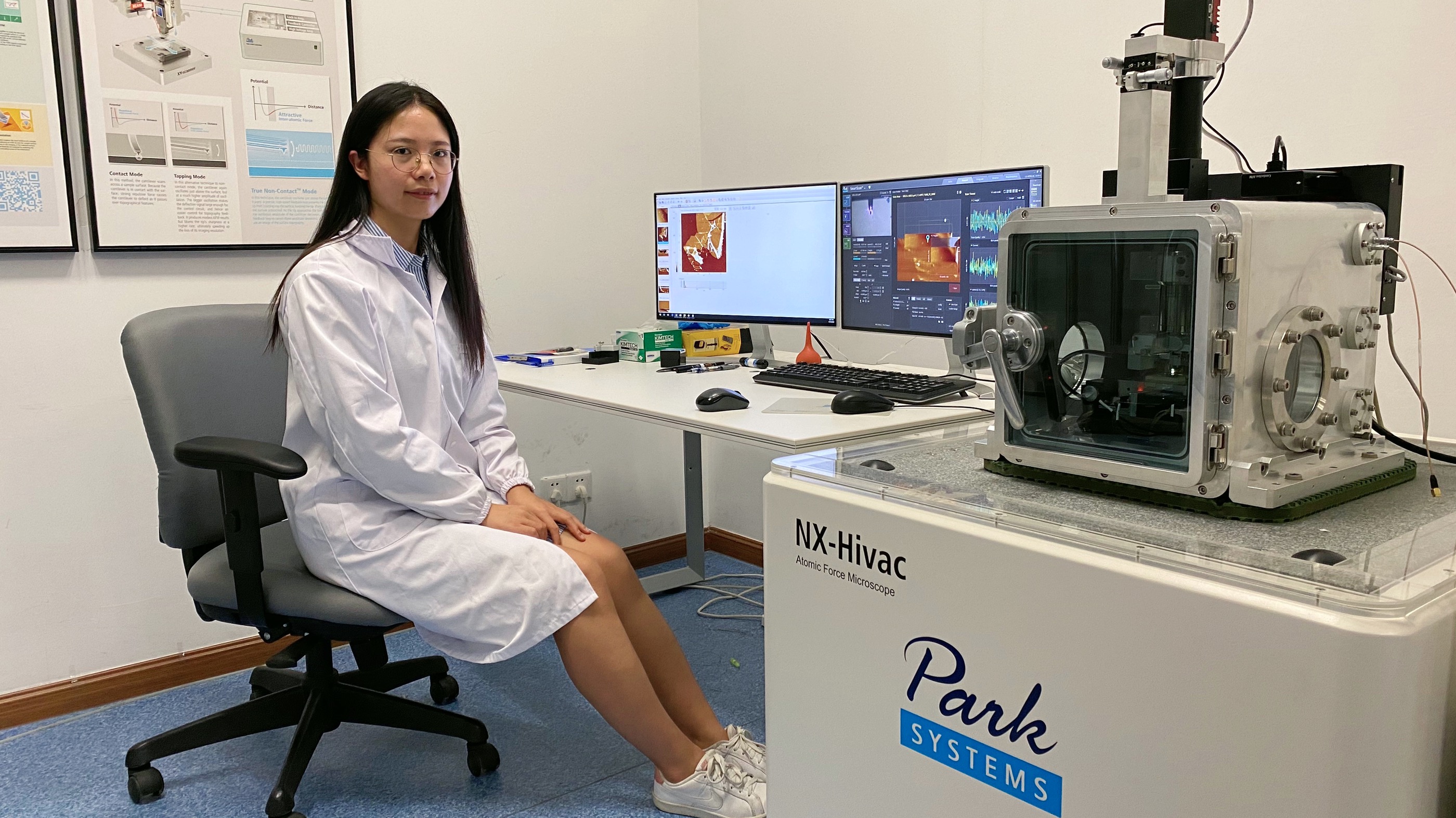
3. What features of Park AFM are the most beneficial and why?
NX-Hivac AFM from Park Systems has two main features which are very important for my experiments. The first feature is that the topography and current maps acquired by this AFM show very small drift even over 20 scans. This is very important because one of my experiments is to analyze the influence of sample bias on the area of the conductive spots in the current map. Only when the drift is very small from one map to another, can we compare the topography and current maps at a specific position. The second important feature is the logarithmic amplifier used in Nx-HiVac AFM. With a linear amplifier, the currents arrive at the saturation level around several nanoamperes. However, this cannot prove the existence of dielectric breakdown in the dielectric layer, which always happens at a current level of microamperes. With a logarithmic amplifier, we can measure the current from picoamperes to milliamperes.
4. Why is the Park AFM important for your research?
My research focuses on the electrical characterization of dielectrics at nanoscale, while CAFM is one of the few tools to realize this goal. When we use CAFM to measure the sample in air, one of the main problems is that a water meniscus forms at the tip/sample junction owing to the ambient humidity. This water layer can increase the effective contact area and the oxidation speed of the sample. Therefore, it is very significant for us to measure the sample under vacuum in order to obtain the intrinsic topographic and electrical information of our sample. With Park Nx-Hivac AFM, we can measure our samples under vacuum condition, as low as to 10-6 torr, which is very important for my research.