


Wednesday, 15 April 2020
- 9:30 am – 10:30 am
(GMT)
London, Dublin - 10:30 am – 12:30 pm
(CEST)
Berlin, Paris, Rome - 17:30pm – 18:30 pm
[UTC+9]
Seoul, Tokyo -

AFM imaging has never been so easy before!
In this Live Demo we will walk you through the quick automation set-up for research applications by using SmartScan & StepScan.
Park SmartScan is an operating software for Park AFMs that allows even less experienced, untrained users producing high quality nanoscale imaging through three simple clicks of a mouse in auto mode. SmartScan manual mode provides all the functions and tools necessary for more seasoned users to feel at home and fully adapt the measurements to their needs.
This combination of extreme versatility, ease-of-use, and quality makes SmartScan the best AFM operating software available.
Park’s StepScan allows for an easy set-up of automated measurements. The areas of interest can be added and edited by a simple mouse click, while the user keeps full control over the measurement at each position. The recipe can vary any parameters like scan size, speed or resolution at any location. Furthermore, modes can also be changed within a StepScan routine, i.e. measuring lateral force microscopy and KPFM during the same recipe.
This allows setting up the system with its full capabilities from manual mode without any restrictions and thus, freeing up the operator’s time as the tool performs the recipe automatically.
Presented By :
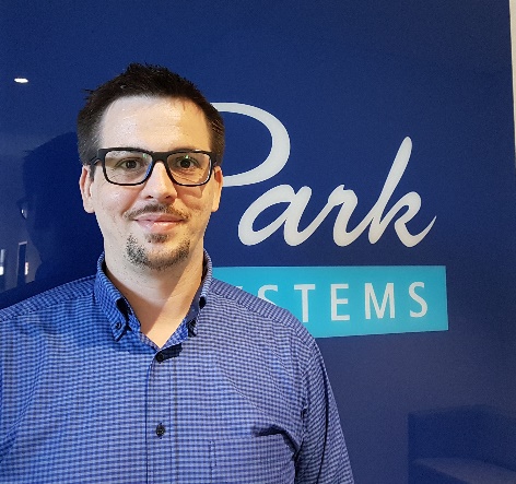
Dr. Florian Stumpf, Application Manager at Park Systems Europe, Mannheim, Germany
fstumpf@parksystems.com
Florian Stumpf is the Application Manager at Park Systems Europe, where he is responsible for the App Team and the measurements of samples or live demos for the research sector. Prior, he worked at the Fraunhofer Institute in Erlangen (Germany) in the group of Mathias Rommel where he was in charge of the AFMs and the communication with Nanoworld. In his position he determined FIB damages and beam tails with Scanning Spreading Resistance Microscopy (SSRM) and Scanning Capacitance Microscopy (SCM). Furthermore, he worked on the development and improvement of a method to determine charge carrier lifetimes in photovoltaic materials with high spatial resolution using Kelvin Probe Force Microscopy (KPFM) and external light sources. During his diploma thesis in nano-sciences he worked on the creation of quantum dots and several methods of characterizing them with an AFM.