Wednesday, 22 April 2020
- 9:30 am – 10:30 am
(GMT)
London, Dublin - 10:30 am – 11:30 am
(CEST)
Berlin, Paris, Rome - 17:30pm – 18:30 pm
[UTC+9]
Seoul, Tokyo -

Learn how automation features in AFM can easily be implemented into your workflow to boost the productivity in your lab.
Our XEA software is designed to acquire accurate and repeatable nanoscale images of target devices according to user-defined procedures in custom recipe files. Utilizing a powerful combination of high-resolution digital CCD camera and pattern recognition software, a fully automated pattern recognition and alignment is made possible for user applications. Through the user-defined recipe, created by combining this optical pattern recognition and the precision of the AFM, accurate and repeatable nanoscale metrology with quantifiable data via automated data acquisition and analysis can be performed.
The corresponding increase in productivity makes this combined software and hardware solution attractive for multiple fields in nano-scaled surface optimization. Fields such as wafer manufacturing (surface roughness) and wafer design research (critical dimension measurement) are two examples of industry and research areas that systematically incorporate a tool capable of fully automated AFM to tune or control their processes and thereby increase the efficiency. Given this ability to automate data acquisition and analysis, this process has a viable application in similar fields.

Presented By :
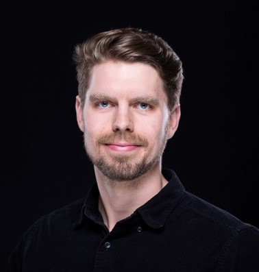
Dr. Victor Bergmann, Application Director at Park Systems Europe, Mannheim, Germany
bergmann@parksystems.com
Victor Bergmann is the Technical Director at Park Systems Europe, where he is leading the team of application and service engineers. Before he joined Park Systems, he spent his PhD at the Max-Planck-Institute for Polymer Research in Mainz in the group of Hans-Jürgen Butt. His main research topic was studying different kinds of solar cells by means of Kelvin Probe Force Microscopy. Within the framework of the International Research Training Group 1404 he also spent half a year at Seoul National University using the AFM to characterize self-organizing nanostructures. As he just recently defended his thesis, he is now waiting for the corona shutdown to end to officially receive his doctoral degree.


