Wednesday, 27 May 2020
- 10:00 am – 11:30 am
(GMT)
London, Dublin - 11:00 am – 12:30 pm
(CEST)
Berlin, Paris, Rome - 17:00 pm - 18.30 pm
(GMT+8)
Beijing, Singapore - 18:00pm – 19:30 pm
(UTC+9)
Seoul, Tokyo

Scanning Capacitance Microscopy (SCM) is a versatile tool in the semiconductor industry for failure analysis and measuring doping profiles with the advantage of being a non-destructive method with high spatial resolution. Applications range from characterizing ion implanted semiconductors, electrical properties of Metal-Oxide-Semiconductor (MOS) devices and non-volatile ultra-high density memories.
In this webinar, we provide an overview and introduction into SCM using a Park Systems NX20 AFM. Furthermore, we will explore the additional options that can be added to traditional SCM using our SmartScanTM Software for improving measurement results and repeatability. First, QuickStepTM allows the user to set a certain holding time at each pixel, which allows for better and more stable tip/sample interaction while scanning the sample. Additionally, the scan speed can be increased to get faster images. Secondly, we will show PinPointTM measuring mode in combination with SCM. PinPointTM is the nanomechanical mode from Park Systems which allows to completely remove the lateral impact of AFM measurements from the electrical scan. This heavily increases the repeatability as the tip/sample interaction is much more controlled and not impacted by lateral movement. Furthermore, nanomechanical properties can be recorded as the same time as the SCM signal is measured.
The SCM setup consists of a conductive (metallic) tip and a highly sensitive capacitance sensor. Together with the oxidized semiconductor the setup forms a MOS capacitor. The capacitance is determined by the oxide layer thickness and the depletion area at the silicon/oxide surface. Thus, with a homogeneous oxide layer the capacitance changes of the sample can be determined by applying an AC bias to the sample.

Presented By :
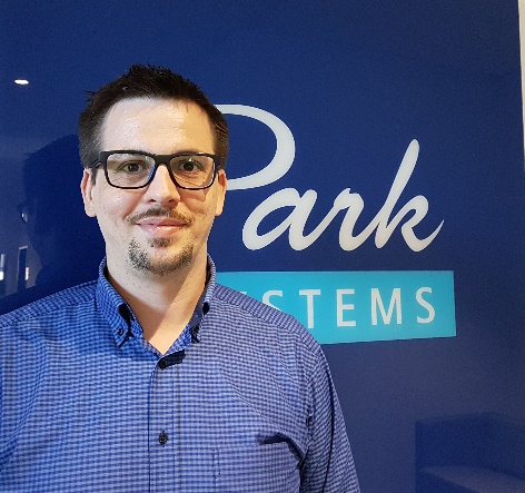
Dr. Florian Stumpf, Application Manager at Park Systems Europe, Mannheim, Germany
fstumpf@parksystems.com
Florian Stumpf is the Application Manager at Park Systems Europe, where he is responsible for the App Team and the measurements of samples or live demos for the research sector. Prior, he worked at the Fraunhofer Institute in Erlangen (Germany) in the group of Mathias Rommel where he was in charge of the AFMs and the communication with Nanoworld. In his position he determined FIB damages and beam tails with Scanning Spreading Resistance Microscopy (SSRM) and Scanning Capacitance Microscopy (SCM). Furthermore, he worked on the development and improvement of a method to determine charge carrier lifetimes in photovoltaic materials with high spatial resolution using Kelvin Probe Force Microscopy (KPFM) and external light sources. During his diploma thesis in nano-sciences he worked on the creation of quantum dots and several methods of characterizing them with an AFM.


