


Friday, May 22, 2020
- 3:00 pm
(EDT)
Boston, New York - 12:00 pm
(PDT)
San Francisco, LA - 8:00 pm
(GMT)
London - 9:00 pm
(CET)
Paris, Rome
Creating nanometer sized structures with ease
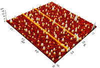
3D image of oxide patterns formed through Park AFM Nanolithography.
Park AFM’s nanolithography is an advanced AFM technique used to pattern nanoscale shapes onto sample surfaces. In the bias-assisted or anodic oxidation method, a bias voltage is applied to the tip to generate an oxide pattern on a metallic or semiconductor substrate. In this session, we will demonstrate how to create nanometer sized structures and discuss the main parameters to consider during the process using SmartScan™ Nanolithography on the Park NX10 AFM system.

Presented By :
Presented by Armando Melgarejo, Park Systems Technical Support Engineer
Armando Melgarejo is an engineer for Park Systems, where he focuses on the installation and support of AFM systems for Park’s research user base. He holds a B.S. in Biotechnology Engineering from Autonomous University of Queretaro, Mexico. During his studies, he also spent a semester doing research in nanotechnology and molecular biology at Czech Technical University in Prague, Czech Republic. Other areas of expertise include diverse characterization techniques (AFM, SEM, RAMAN and IR), genetics and molecular and cell biology.