


Tuesday, 20 October, 2020
- 13:30 pm
(SGT)
Singapore - 10:30 am
(PKT)
Islamabad, Pakistan - 11:00 am
(IST)
Bangalore, India - 16:30 pm
(AEDT)
Sydney, Australia

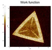
- Quantitative nanoscale potential/work function measurements as well as topography using KPFM
- Sample: CVD grown WS2 on SiO2
- AFM mode: KPFM
Since atomic force microscopy (AFM) has been developed, it becomes novel technique for surface investigation including topography and other material properties measurement. AFM shows high utilization in the research field due to complementary relationships with optical microscopy, electron microscopy and other measuring equipment.
In this session, a variety of AFM option mode is introduced for investigating sample’s properties such as electrical, mechanical, magnetic, thermal and electrochemical properties. Based on Contact or Non-contact mode, AFM option mode can be combined to monitor sample’s properties as well as topography. Also, we highlight the applications and representative images at each option mode to help your understanding about AFM option mode. The goal of this session is not only introducing the AFM option mode, but also to let you know how AFM can help your research or sample.
After oral session, AFM – Kelvin probe force microscopy (KPFM), one of the AFM option mode for electrical property measurement, live demo is prepared by Park Systems skillful engineer. During the AFM live demo session, hardware and software setup of KPFM are presented for understanding of actual AFM option mode measurement.
Presented By :
Jake Kim, Application Technology Center Manager, Park Systems
Dr. Kim received Ph.D. degree in Materials Science and Engineering from Nanyang Technological University, Singapore. He joined Tokyo Institute of Technology International Research Opportunities Program (TiROP) in 2014 and was engaged in nano-scale chemical composition analysis using scanning probe microscopy (SPM). From December 2017, he started to work in Park Systems as the manager of application technology center. He is specialized in the enhancement of nano-machanical measurement performance for Atomic Force Microscopy (AFM), building up a accurate and reliable environment for electrochemical measurement using Scanning Probe Microscopy (SPM; SECM,SECCM) and Scanning Ion Conductance Microscopy (SICM) applications development for biology.