Make the most out of your tip: the benefits of True Non-contact mode imaging
5 May, 2021
- 10:00 am – 11:30 am
(GMT)
London, Dublin - 11:00 am – 12:30 pm
(CET)
Berlin, Paris, Rome - 17:00 am – 18:30 pm
[GMT+8]
Beijing, Singapore - 18:00pm – 19:30 pm
[UTC+9]
Seoul, Tokyo

Abstract:
For topographical imaging most atomic force microscopes (AFMs) rely on intermittent or tapping mode. This technique oscillates the AFM probe at a driving frequency close to its resonance frequency with amplitudes in the tens or hundreds of nanometers. At each pixel the tip comes into intermittent contact with the sample and the change in amplitude provides the height signal.
The downside of tapping mode is the actual contact between sample and tip as this will lead to tip wear or even sample damage of soft material during the scan. This does not only reduce the lifetime of the tip and thus, the cost of ownership of the AFM, but can also decrease image quality due to changes of tip shape.
This issue is tackled by the True Non-Contact Mode (NCM) on the Park Systems’ tools. Here, the tip is oscillated at lower amplitudes and not brought into contact with the sample by working only in the attractive regime of the Lennard-Jones-Potential.
In this webinar we present on how to setup Tapping Mode and NCM on our tool and how to differentiate between those modes during a live scan. Furthermore, we will show results that emphasize the benefit of NCM compared to Tapping Mode.

Presented By :
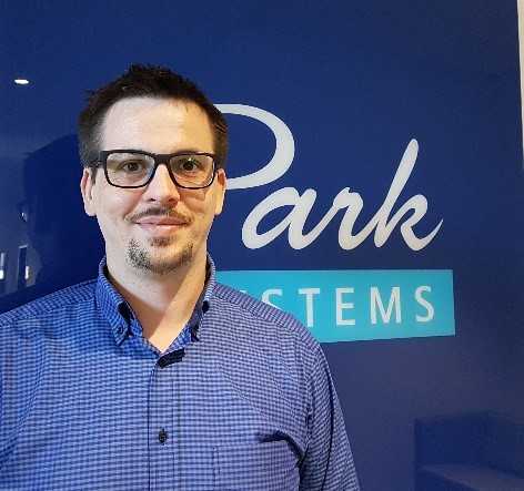
Dr. Florian Stumpf, Application Manager at Park Systems Europe, Mannheim, Germany
fstumpf@parksystems.com
Florian Stumpf is the Application Manager at Park Systems Europe, where he is responsible for the App Team and the measurements of samples or live demos for the research sector. Prior, he worked at the Fraunhofer Institute in Erlangen (Germany) in the group of Mathias Rommel where he was in charge of the AFMs and the communication with Nanoworld. In his position he determined FIB damages and beam tails with Scanning Spreading Resistance Microscopy (SSRM) and Scanning Capacitance Microscopy (SCM). Furthermore, he worked on the development and improvement of a method to determine charge carrier lifetimes in photovoltaic materials with high spatial resolution using Kelvin Probe Force Microscopy (KPFM) and external light sources. During his diploma thesis in nano-sciences he worked on the creation of quantum dots and several methods of characterizing them with an AFM.


