


-
ScanningTunnelingMicroscopy Yeditepe_University Ananth Indent Lateral_Force_Microscopy Logo OpticalWaveguides TungstenThinFilmDeposition PetruPoni_Institute SurfaceChange Ca10(PO4)6(OH)2 Chloroform IndiumTinOxide CeNSE_IISc alkanes PolyvinylAcetate Ferroelectric Magnetostrictive FM-KPFM AM_SKPM Tape TiO2 StrontiumTitanate PyroelectricDetector Ito Moire TemperatureControl ConductingPolymer Nickel 3-hexylthiophene Ni-FeAlloy doped lithography Croatia NCM
Report image
If you found this image unacceptable, please let us know. We will review your report and take action if we determine this image is really unacceptable.
AlN/GaN/AlN Hetero Structure
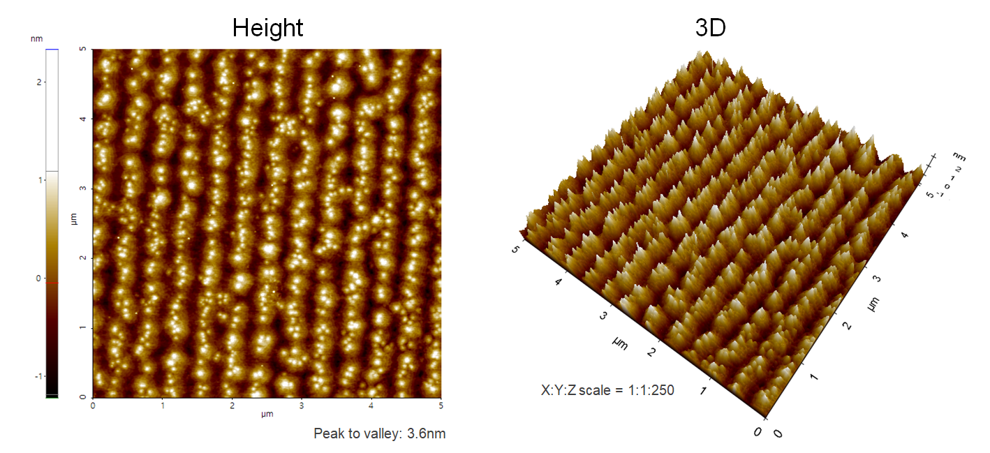
AlN/GaN/AlN hetero structure grown on SiC substrate by Molecular Beam Epitaxy (MBE) system.
Scanning Conditions
- System: NX20
- Scan Mode: Non-contact
- Cantilever: AC160TS (k=26N/m, f=300kHz)
- Scan Size: 5μm×5μm
- Scan Rate: 0.5Hz
- Pixel Size: 512 × 512
- Scan Mode: Non-contact
- Cantilever: AC160TS (k=26N/m, f=300kHz)
- Scan Size: 5μm×5μm
- Scan Rate: 0.5Hz
- Pixel Size: 512 × 512