


-
Polyaniline TempControl HBN Step Piezoelectric Pores ContactModeDots Nanotechnology #Materials UTEM Conducting PinpointNanomechanicalMode LifeScience temperature_control MultiLayerCeramicCapacitor NUS_NNI_Nanocore UnivMaryland MagneticPhase fluoroalkane Kevlar ThermalConductivity INSP HexacontaneFilm SingleLayer 2d_materials Writing ForceVolumeImage polymeric_arrays Yeditepe_University Growing SKKU Reading ElectroDeposition Bio AnodizedAluminumOxide
Report image
If you found this image unacceptable, please let us know. We will review your report and take action if we determine this image is really unacceptable.
Fe Thin Films
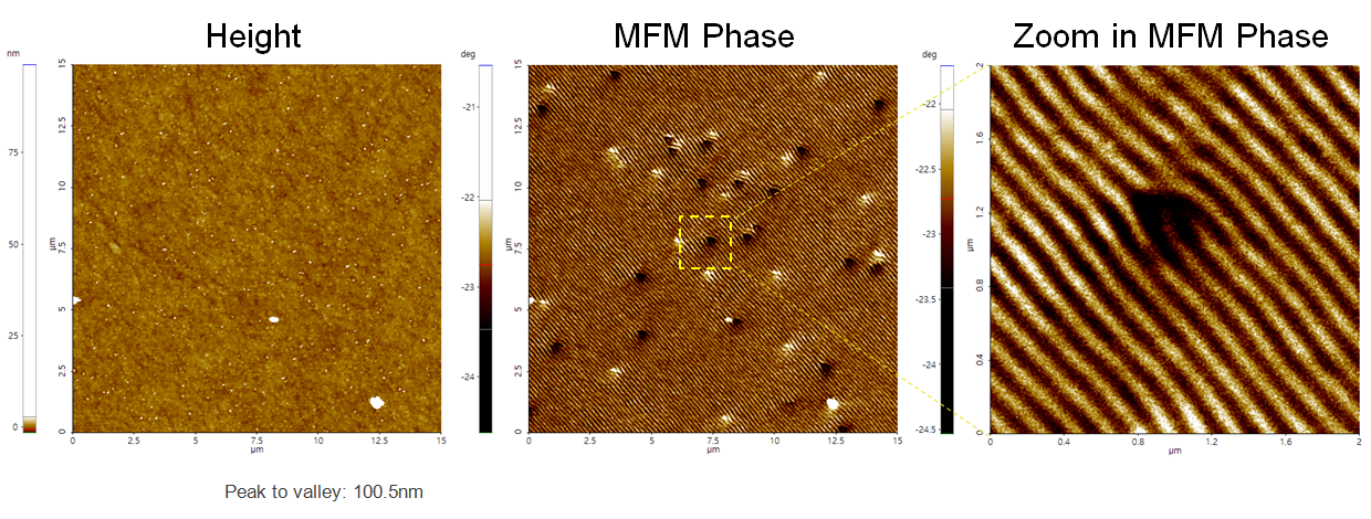
MFM images of Fe thin films (80 nm) epitaxied on GaAs(001) and then implanted with N-atoms. Images reveal weak stripe domains at magnetic remanence.
Scanning Conditions
- System: NX10
- Scan Mode: MFM
- Cantilever: PPP-MFMR (k=2.8N/m, f=75kHz)
- Scan Size: 15μm×15μm,2μm×2μm
- Scan Rate: 0.5Hz, 1Hz
- Pixel Size: 512×512, 256×256
- Lift height: 50nm
- Scan Mode: MFM
- Cantilever: PPP-MFMR (k=2.8N/m, f=75kHz)
- Scan Size: 15μm×15μm,2μm×2μm
- Scan Rate: 0.5Hz, 1Hz
- Pixel Size: 512×512, 256×256
- Lift height: 50nm