


-
NCM\ Electrode Phosphide Fluoride TCS AIN Materials self-assembly MagneticForceMicroscopy Au111 NeodymiumMagnets WPlug Genetic Perovskite Heat SolarCell Ceramic Kevlar LiNbO3 DOE MechanicalProperty Force-distance Piezo STM Indium_tin_oxide SiWafer Techcomp Fet semifluorinated alkane Hexacontane vertical_PFM atomic_layer Edwin Chromium pulsed_laser_deposition
Report image
If you found this image unacceptable, please let us know. We will review your report and take action if we determine this image is really unacceptable.
Taegeuk Mark Lithography on PZT
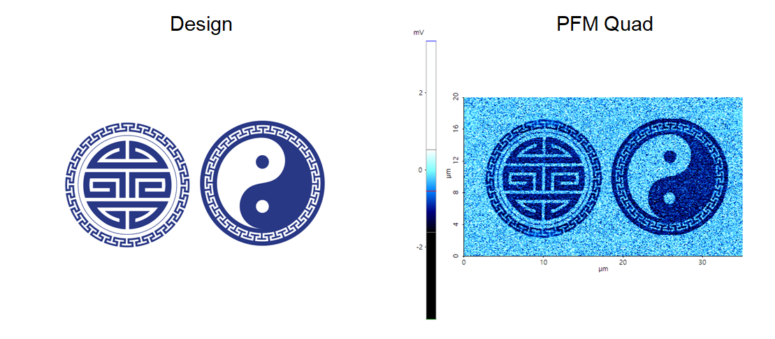
Re-arranged the domain pole direction on PZT surface using bias mode of lithography.
Scanning Conditions
- System: NX10
- Scan Mode: Lithography
- Cantilever: PPP-ContScPt (k=0.2N/m, f=25kHz)
- Scan Size: 35μm×20μm
- Scan Rate: 0.5Hz
- Pixel Size: 1024 × 1024
- Tip Bias: 10V for patterned area
- Scan Mode: Lithography
- Cantilever: PPP-ContScPt (k=0.2N/m, f=25kHz)
- Scan Size: 35μm×20μm
- Scan Rate: 0.5Hz
- Pixel Size: 1024 × 1024
- Tip Bias: 10V for patterned area