


-
LFM TungstenThinFilmDeposition polyvinyl acetate norganic H-BN Electronics Beads Fendb KPFM Wang Piezo LiBattery Conductance FM-KPFM Polarization mono_layer tip_bias_mode Yttria_stabilized_Zirconia ItoGlass IISCBangalore C36H74 BFO OpticalWaveguide IMT_Bucharest CuParticle Protein BiasMode Yeditepe_University Subhajjit BiVO4 self-assembly alkanes Hafnia HanyangUniv Inorganic_Compound
Report image
If you found this image unacceptable, please let us know. We will review your report and take action if we determine this image is really unacceptable.
Monolayer Graphene on PDMS Surface
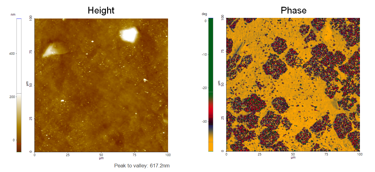
Monolayer Graphene grown on Cu foil using CVD process is transferred on to PDMS substrate.
Scanning Conditions
- System: NX20
- Scan Mode: Tapping
- Cantilever: Access-NC (k=113N/m, f=330kHz)
- Scan Size: 100μm×100μm
- Scan Rate: 0.6Hz
- Pixel Size: 256 × 256
- Scan Mode: Tapping
- Cantilever: Access-NC (k=113N/m, f=330kHz)
- Scan Size: 100μm×100μm
- Scan Rate: 0.6Hz
- Pixel Size: 256 × 256