Electrical Modes
PinPoint™ AFM Nanoelectrical Modes

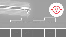
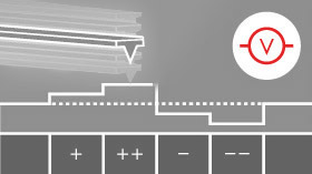
PinPointTM nanoelectrical modes eliminate lateral shear forces between the cantilever tip and the surface, thus minimizing damage while ensuring high imaging quality and reproducibility for a wide range of samples over many consecutive measurements. PinPoint can be combined with other AFM modes to obtain information about electrical properties such as:
• PinPoint Conductive AFM (C-AFM)
• PinPoint Piezoresponse Force Microscopy (PFM)
• PinPoint Scanning Spreading Resistance Microscopy (SSRM)
Brochures
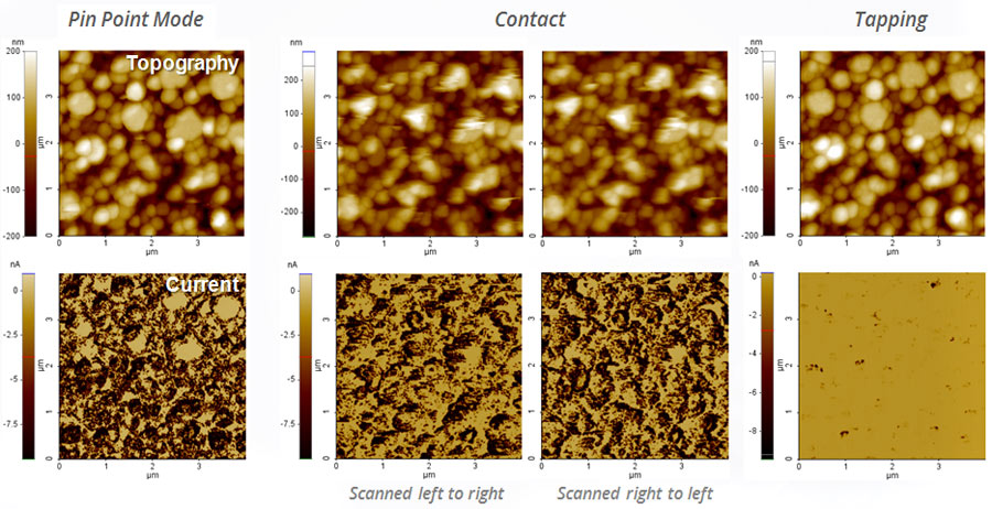
PinPoint™ Conductive AFM obtains the best of resolution and sensitivity during current measurements
PinPoint™ Conductive AFM was developed for well defined electric contact between the tip and the sample. They XY scanner stops while measuring the electric current with contact time controlled by a user. PinPoint™ Conductive AFM allows higher spatial resolution, without lateral force, with optimized current measurement over different sample surface.
Learn more about how PinPoint mode enhances investigation of electrical and electromechanical properties here
Conductive AFM (C-AFM)

Probing the Local Electronic Structure of a Sample’s Surface
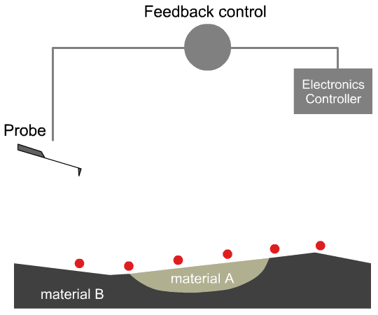
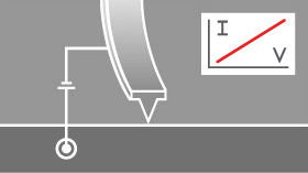
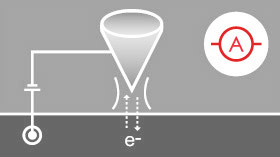
With the continuous decrease in device sizes and critical dimensions in the semiconductor industry, the ability to measure electrical properties locally with a high spatial resolution is vital for accurate device characterization and failure analysis. Here, Atomic force microscopy (AFM) offers real space imaging of local surface properties on the nanoscale. Conductive AFM (C-AFM) in particular, simultaneously measures the topography and conductivity of a sample by scanning the surface with a conductive material coated tip as a nanoscale electrical probe at an applied DC bias.
Read More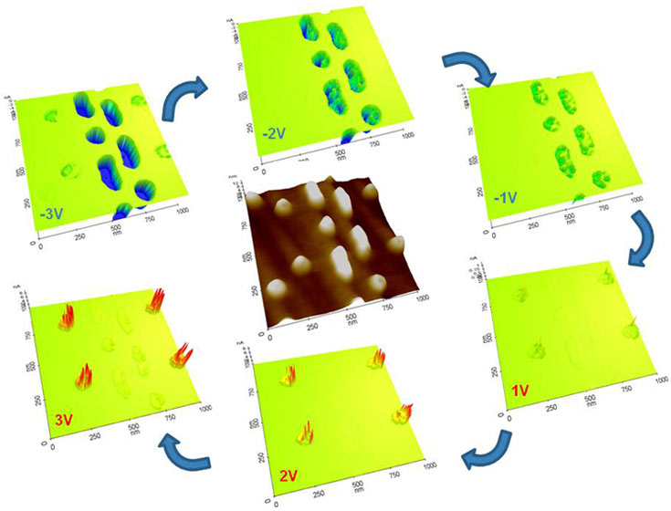
I-V Spectroscopy
Park AFMs feature the ability to conduct current voltage spectroscopy on specified point of the sample surface. The low noise of Park Systems’ conductive AFM options allows for the detection of extremely small changes in a sample’s electronic characteristics.
Read More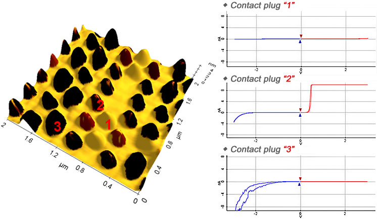
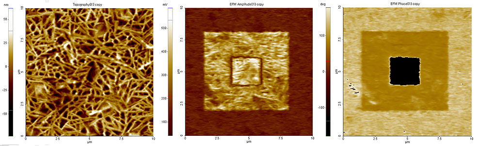
Electrostatic Force Microscopy (EFM)
High Resolution and High Sensitivity Imaging of Electrostatic Force
Almost every surface property measured by AFM is acquired by the process depicted. EFM measurements follow the same procedure. For EFM, the sample surface properties would be electrical properties and the interaction force will be the electrostatic force between the biased tip and sample. However, in addition to the electrostatic force, the van der Waals forces between the tip and the sample surface are always present. The magnitude of these van der Waals forces change according to the tip-sample distance, and are therefore used to measure the surface topography.
Read More
Kelvin Probe Force Microscopy (KPFM)
High Resolution and High Sensitivity Imaging of Surface Potential
Principle of KPFM is similar to Enhanced EFM with DC bias feedback. DC bias is controlled by feedback loop to zero the ω term. The DC bias that zeros the force is a measure of the surface potential. The difference is in the way the signal obtained from the Lock-in Amplifier is processed. As presented in previous section, the ω signal from Lock-in Amplifier can be expressed as following equation. scanning-kelvin-probe-microscopy-KPFM-f3 The ω signal can be used on its own to measure the surface potential. The amplitude of the ω signal is zero when VDC = Vs, or when the DC offset bias matches the surface potential of the sample. A feedback loop can be added to the system and vary the DC offset bias such that the output of the Lock-in Amplifier that measures the ω signal is zero. This value of the DC offset bias that zeroes the ω signal is then a measure of the surface potential. An image created from this variation in the DC offset bias is given as an image representing the absolute value of the surface potential.
Read More
Dynamic Contact EFM (DC-EFM)
High Resolution and High Sensitivity Imaging of Electrostatic Force
DC-EFM is capable of extremely high definition EFM results. Patented by Park Systems, DC-EFM actively applies an AC voltage bias to the cantilever and detects the amplitude and the phase change of the cantilever modulation with respect to the applied bias. DC-EFM provides the ability to monitor the second harmonic of the modulation which can be compared to the capacitance of a sample and enhances the electric force signal from the background intermolecular force.
Read More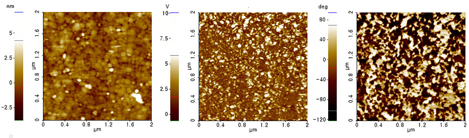
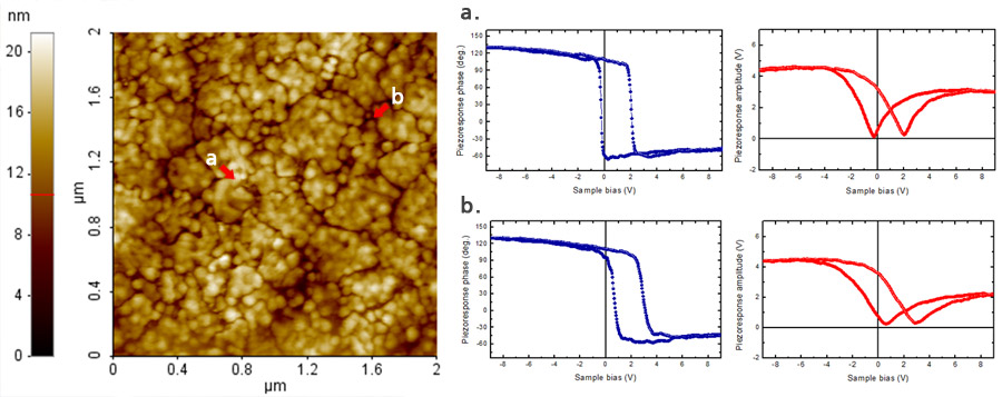
Piezoresponse Force Microscopy (PFM)
Piezoresponse force microscopy (PFM) is a functional Atomic force microscopy (AFM) mode, which probes electromechanical material properties on the nanometer scale in addition to the sample topography. As a conductive tip scans the surface in contact, an AC voltage introduces an electromechanical response in piezoelectric compounds and thereby resolves local variations of piezoelectric and ferroelectric properties. PFM has gained increasing recognition for the unique information it can offer on the electromechanical coupling characteristics of various materials including actuators, sensors, and capacitors for modern communication technology.
Read More
Piezoresponse Force Spectroscopy
Our Piezoresponse Force Spectroscopy mode measures the local amplitude/phase response to a DC bias between tip and sample surface. The polarity of local piezoelectric domain switches depend on the sign and amount of applied voltage.
QuickStep™ SCM
 In QuickStep scan, the XY scanner stops at each pixel point to record the data. It makes a fast jump between the pixel points.
QuickStep™ to make faster SCM data acquisition
In order to improve the signal-to-noise ratio, conventional SCM adopts very slow scan speeds as a means of giving the detector enough time to collect the data. QuickStep™ SCM differs from the conventional methodology of slow continuous movement. Here, XY scanner stops at each pixel point to record the data and then makes a fast and rapid hop to the next measurement points. This effectively speeds up the scan rate while maintaining the same signal sensitivity of the measurements by conventional SCM at slow scan speeds.
Application note: Accurate dopant profiles of semiconductor device structures with QuickStep Scanning Capacitance Microscopy
 QuickStep Scan (Scan rate 1.5Hz)
 Conventional Scan (Scan rate 1Hz)
Scanning Capacitance Microscopy (SCM)

High Resolution and High Sensitivity Imaging of Charge Distribution
Our SCM mode provides doping concentration information over the sample surface by measuring the capacitance change between tip and sample. the module enables a variable resonator frequency, which allows a wide RF bandwidth capable of monitoring a large range of doping concentrations by selecting the most sensitive frequency of the resonator for a specific doping range.
Read More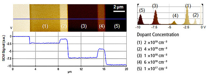
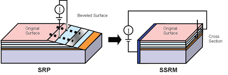
Scanning Spreading Resistance Microscopy (SSRM)

Probing the Local Electronic Structure of a Sample’s Surface
Our SSRM mode precisely measures the local resistance over a sample surface by using a conductive AFM tip to scan a small region while applying DC bias.
Read More
Scanning Tunneling Microscopy (STM)
Probing the Local Electronic Structure of a Sample’s Surface
STM measures the tunneling current between tip and sample, giving highly accurate sub-nanometer scale images you can use to gain insights into sample properties.
Read More
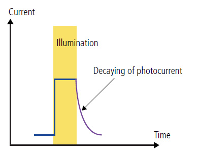
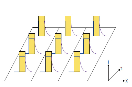
Photo Current Mapping (PCM)

Enabling Innovation in Photosensitive Materials Research
Our PCM mode measures photoelectric response to a illumination without interference from unwanted light sources, including the feedback laser. This mode features a laser illumination module and acquisition and analysis software.
Read More