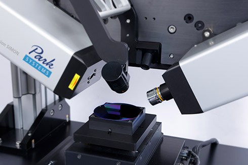
FX40 with monitor

Accurion SIMON

Your Entry to Imaging Ellipsometry

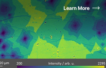
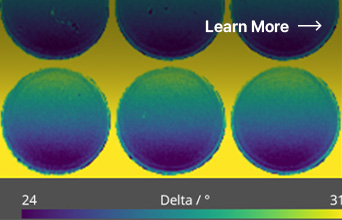
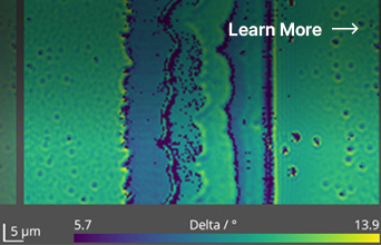
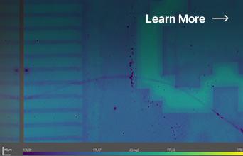
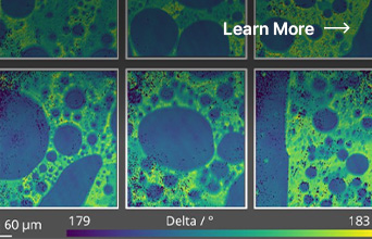
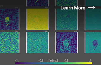
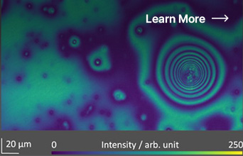
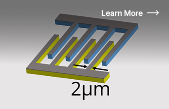
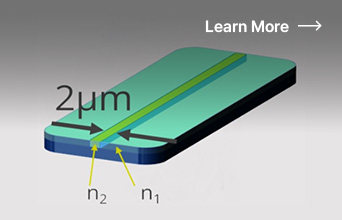
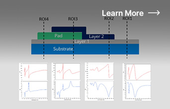
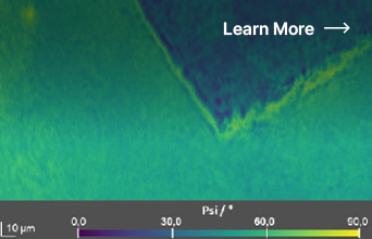
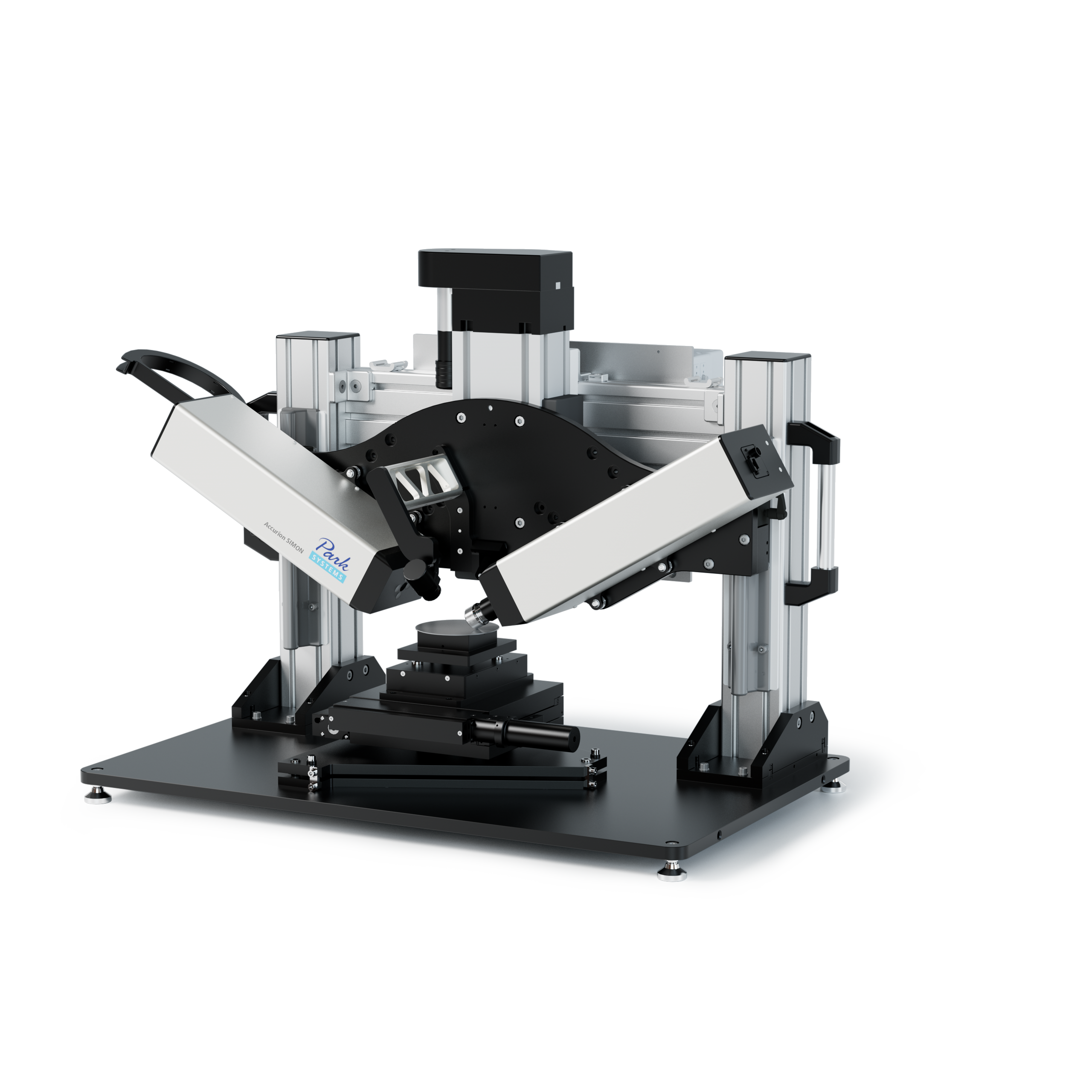
SIMON is specifically designed for routine measurement tasks. Its simple user interface and robustness of a fixed angle ellipsometer enables the entry to imaging ellipsometry. It can be operated in two different modes. The microscopic mode is very fast and allows to visualize variations and defects in thinnest layers (e.g. monolayers: d = 0.35 nm), whereas the ellipsometric mode measures thickness and the refractive index of the sample materials. Imaging Ellipsometry itself combines the sensitivity of thickness and refractive index measurements with the imaging of microscopy. This allows determining thickness and refractive index variations with microscopic images on e.g. micro-structured samples. Typical applications include the surface inspection of homogeneities and defects of large samples in quality control or the fast localization of flakes of 2D Materials.

Surface Inspection Metrology of Nanofilms

Typical Applications: Large Area Inspection and Automatic Flakesearch

SIMON is designed to automatically stitch large areas with smooth transitions. A complete 4” wafer can be inspected within 47 minutes, whilst observing defects, particles and inhomogoneities as small as 10 μm. SIMON also allows searching for flakes or materials with desired thicknesses. Through the imaging aspect of SIMON, histogram analysis on a single measurement becomes possible and provides a detailed insight into the distribution of thicknesses or inhomogeneities.

Thickness and Refractive Index Measurements of Microstructures

The combination of ellipsometry and microscopy allows to measure the thickness maps of your sample. These maps are comparable to AFM measurements, but can also be measured for non top layers. Additionally, imaging ellipsometry will measure the thickness map of approx.500 μm (X) x 550 μm (Y) in less than 1 minute. The thickness resolution is below 0.01 nm within a range of 0.01 nm < d < 5 μm*. The ellipsometric mode also determines the refractive index. This allows users to determine refractive index variation, that e.g. occurs in holographic gratings scribed by a laser. Small changes in refractive index, as for example seen in waveguides, can thus be visualized and observed. *Depending on sample/substrate combination

Key Features

  • Easy to use entry level system
  • Imaging Ellipsometry with a lateral ellipsometric resolution down to 1 µm
  • Thickness and refractive index measurements of microstructures
  • Fast visualization of layer thickness distribution and hidden defects on large areas

Applications

aaa

2D-Materials

Imaging spectroscopic ellipsometry characterizes graphene and other 2D materials, analyzing CVD grown, exfoliated, and epitaxially grown flakes with the ep4 ellipsometer.

aaa

Curved Surfaces

Ellipsometry measures thin films and AR coatings on flat and curved surfaces. The ep4 ellipsometer addresses AR coating issues on micro-lens arrays.

aaa

Transparent Substrate

Thin films on transparent substrates are key for flexible displays. Knife edge illumination suppresses reflections, allowing non-destructive examination.

aaa

Surface Engineering

Silanization bonds mineral/inorganic and organic components in paints and adhesives. Imaging ellipsometry examines bond formation in structured arrays without fluorescence markers.

aaa

Air-Water Interface

The air/water interface is crucial in biophysics and industry. Brewster angle microscopy (BAM) visualizes Langmuir-Blodgett monolayers and biological materials, investigating molecules, proteins, drugs, DNA, and nanoparticles.

aaa

Anisotropic Films

Anisotropic micro crystals are promising for electronics. Imaging Mueller Matrix Ellipsometry (IMME) measures refractive indices and optical axis orientation in anisotropic thin-film samples like Black Phosphorous.

aaa

Bio Interfaces

Imaging Ellipsometry (IE) provides high sensitivity for mono- and sub-monolayer thickness. It offers micromaps of ellipsometric angles and a contrast mode for thickness changes. Accessories like cells and QCM-D enhance its biological application capabilities.

aaa

MEMS

Spectroscopic ellipsometry measures MEMS structures as small as 1µm, with 0.1nm film thickness resolution. A single measurement provides thickness, refractive index, composition, and contaminations. ECM mode allows fast quality control and curved surface measurements.

aaa

Photonics

Spectroscopic ellipsometry measures optical fibers and waveguides with 1µm lateral resolution and 0.1nm thickness resolution. It covers 190nm to 1700nm, extendable to 2700nm, providing optical data and fast quality control.

aaa

Displays

Spectroscopic measurements on micron-scale regions use the ROI concept for multiple measurements in one run. The UV range down to 190nm characterizes display materials. A single measurement provides thickness, dispersions, and compositions, with RCE6 mode allowing sub-20-second tact times.

aaa

Battery Materials

Operando Imaging Ellipsometry monitors battery electrode materials during charging and discharging, measuring microscopic maps of Delta and Psi. It provides data from various regions, with post-processing analysis including profiles, sub-region, and histogram analysis.