FX40 with monitor

Dynamic Contact EFM (DC-EFM)

DC-EFM is capable of extremely high definition EFM results. Patented by Park Systems, DC-EFM actively applies an AC voltage bias to the cantilever and detects the amplitude and the phase change of the cantilever modulation with respect to the applied bias. DC-EFM provides the ability to monitor the second harmonic of the modulation which can be compared to the capacitance of a sample and enhances the electric force signal from the background intermolecular force.

Unique Enhanced EFM Capabilities Provided Only by the Park AFM

High Resolution and High Sensitivity Imaging of Electrostatic Force

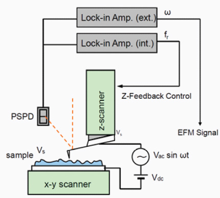
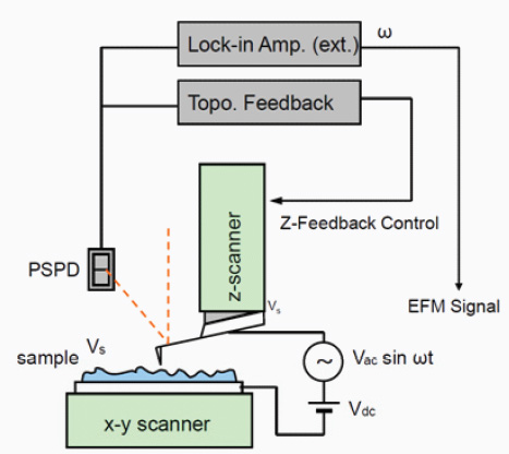
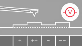
For Electrostatic Force Microscopy (EFM), the sample surface properties investigated are electrical in nature and the interaction force used will be the electrostatic force between a biased tip and sample. However, in addition to the electrostatic force, the van der Waals forces between the tip and the sample surface are always present. The magnitude of these van der Waals forces change according to the tip-sample distance and are therefore used to measure the surface topography. Hence the obtained signal contains both information for both surface topography and surface electrical properties generated by the van der Waals and electrostatic forces respectively. The key to successful EFM imaging lies in the separation of the EFM signal, the information regarding surface electrical properties, from the entire signal. EFM modes can be classified according to the method used to separate the EFM signal.

Enhanced EFM

Three extra EFM modes are supported by the Enhanced EFM (optional for XE Series) for Park AFM. They are Dynamic Contact Electrostatic Force Microscopy (DC-EFM), Piezoelectric Force Microscopy (PFM), and Kelvin Probe Force Microscopy (KPFM). DC-EFM, patented by Park Systems under US Patent 6,185,991, and PFM are largely identical techniques. KPFM is also known as Surface Potential Microscopy. The schematic diagram of Enhanced EFM for Park AFM is shown in Figure 1. An external lock-in amplifier is connected to the Park AFM for two purposes. One is to apply an AC bias of frequency (ω) to the tip in addition to the DC bias being applied by the Park AFM controller. The other purpose is to separate the frequency (ω) component from the output signal. This unique capability offered only through the Enhanced EFM is what distinguishes it from the standard EFM hardware for Park AFM.


• Surface charge distribution and potential imaging
• Failure analysis in micro electronics circuitry
• Mechanical hardness measurement (DC-EFM)
• Charge densitometry for ferroelectric domain
• Voltage drop on microresistors
• Work function of a semiconductor

DC-EFM

Figure 3. Schematic diagram of the Dynamic Contact EFM (DC-EFM) of the Park AFM. The unique EFM capabilities are patented and provided only by Park Systems.

DC-EFM is a mode enabled through the use of the Enhanced EFM for Park AFM that operates in Contact mode, providing much improved spatial resolution and more sensitive detection (see Figure 3). Figure 4 compares topography and surface charge images of a TGS single crystal acquired by DC-EFM (upper row) and conventional EFM (lower row). The EFM image taken with conventional EFM shows strong coupling of the topography signal to the image while the image taken with DC-EFM shows complete separation of the topography. The key advantages of DC-EFM are as follows: The schematic diagram of Enhanced EFM for Park AFM is shown in Figure 1. An external lock-in amplifier is connected to the Park AFM for two purposes. One is to apply an AC bias of frequency (ω) to the tip in addition to the DC bias being applied by the Park AFM controller. The other purpose is to separate the frequency (ω) component from the output signal. This unique capability offered only through the Enhanced EFM is what distinguishes it from the standard EFM hardware for Park AFM.


• No need of special sample treatment
• High spatial resolution and noninvasive probing.
• Simultaneous topography and domain imaging (Figure 2)
• Real-time imaging of domain dynamics
• Nanoscale control and visualization of domains (Figure 5)
• Detailed local information rather than integral effect

Figure 4. (a) Topography and (b) surface charge image of TGS single crystal by DC-EFM and (c) topography and (d) surface charge image by conventional EFM.

Figure 5. (a) Domain switching behavior in ferroelectric materials. Creation of small domains of TGS by (b) positive applied voltage of 10 V, and (c) negative applied voltage of 10 V.