


展示会

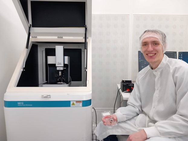
Simon Salleh Atri is a PhD student at the Tel Aviv University, Faculty of Exact Sciences, where he also achieved his bachelor’s (2016-2019) and master’s (2019-2021) degree in physics. As a Laboratory and Research Assistant to Dr. Moshe Ben Shalom, he focused on polarization in graphene polytypes and Electrical-induced stack switching in MoS2 and graphene polytypes. His current research is aimed at the study of the unique properties that arise when Van der Walls layered materials are stacked into different polytypes (recently called Van der Walls Polytypes) and why this occurs.
1. Please summarize the research you do and explain why it is significant?
Multi-layer graphene can be stacked in different polytypes, each with unique properties as shown in trilayer rhombohedral graphene, where orbital-magnetism and superconductivity were found. In the four-layer case, there are three possible polytypes, Bernal (ABAB), Rhombohedral (ABCA), and ABCB, from which only the latter has a polar axis and a non-centrosymmetric unit cell, the necessary conditions for the existence of electrical polarization.
In this project we show that electrical polarization indeed arises in this polytype, study its behavior under electrostatic doping, and use theoretical tools to understand its source.
Contrary to other ferroelectric and polar materials, this multilayer is composed of only one kind of atom (Carbon), thus the study of electrical polarization here helps to understand fundamentally the existence of polarization and the spatial distribution of electrons within the crystal (or why would polarization arise in such a system). Additionally, we observe for the first time that the addition of charge carriers (holes in this case) increases the value of the polarization rather than decreasing it, as would be normally expected.
2. How might your research be used?
My research focuses mainly on the fundamental properties of the different polytypes of multi-layer graphene. Understanding why the properties change and how electron correlations depend on the crystal stacking is important in terms of fundamental physics. Additionally, learning how to switch between polytypes is appealing from a technological point of view, since it will allow one to choose a desired property just by switching the stack of the multilayer.
3. Why is the Park AFM important for your research?
Two-dimensional layered materials have by definition a very small thickness compared to their spanning area; Park AFM becomes a natural tool for their study since it allows one to measure different quantities over the sample area, including, topography, piezo, magnetic, and electrostatic response.
When studying Van der Walls polytypes, apart from learning how those properties change with the stacking sequence, measuring and mapping those quantities helps us to characterize and understand which polytype we are dealing with before further studies, it is then an essential step in our research.
4. What features of Park AFM are the most beneficial and why?
We work with NX10 and the HIVAC system:
- User-friendly interface that allows scanning in a fast way
- Versatility: it is easy to change the operating mode, and there are many to choose
- Real non-contact mode: Allows longer tip life and avoids damaging the sample, which is very important for us when dealing with quasi-equilibrium polytypes that can disappear with contact or tapping mode
- Sideband KPFM: allows high spatial resolution and a low noise KP signal, which was essential to measure the electrical polarization of ABCB graphene, it allowed us to see a 3 mV step between polytypes
- Working in a high vacuum with HIVAC is essential to measure electrostatic properties in our materials.
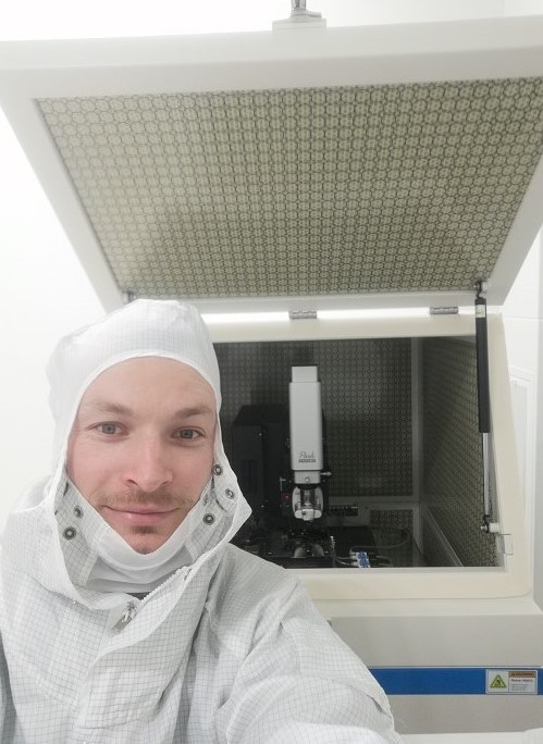
Jori Schmidt is currently enrolled as a master’s student at the Technische Universität Dresden, where he also received his BSc. Degree in the group of Prof. Lukas M. Eng. The title of the thesis was “Towards 3D magnetic force microscopy”, where he used the NX10 AFM by Park Systems to experiment with a new way of performing lateral MFM measurements. Currently, he is continuing his investigations into magnetic domain imaging.
1. Please summarize the research you do and explain why it is significant?
I have performed magnetic force microscopy and shown that using a custom tip-holder, it is possible to use a torsional cantilever oscillation to image in-plane magnetic field components. This signal is sensitive to the in-plane directions of the magnetic stray field and can therefore provide more information about it. It was even possible to simultaneously record a conventional MFM signal at the same time by exciting the cantilever in both its flexural and torsional modes simultaneously.
2. How might your research be used?
One goal would be to better understand the nature of more complicated magnetic structures, such as skyrmions and antiskyrmions.
3. Why is the Park AFM important for your research?
It makes it easy to experiment with new imaging modes due to its flexible IO and software. The conventional MFM imaging mode works very well and is a great foundation to build upon.
4. What features of Park AFM are the most beneficial and why?
The IO module which lets the user get access to all signals of the AFM and allows external control of some functions made implementation of the new imaging mode very easy. Via the aux-inputs, external signals can be read in as a custom data channel which is very helpful. In the software, the options to change parameters during the second pass (such as turning off the NCM drive) also proved useful.
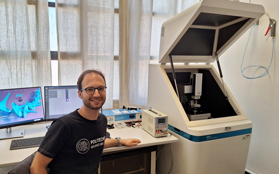
Valerio Levati is a Ph.D. student at the Physics Department of Politecnico di Milano. He received both his B.Sc. and M.Sc. in Engineering Physics from the same university, where he then joined the PhyND group led by Prof. Daniela Petti and Prof. Edoardo Albisetti. His current research project deals with advanced nanofabrication for spintronics and nanoelectronics, aiming at developing innovative methods for crafting the physical properties of nanostructured materials by means of Phase Nanoengineering.
1. Please summarize the research you do and explain why it is significant.
My research is focused on tailoring the physical properties of quantum materials and artificial nanostructures by inducing local tunable modifications on low dimensional systems through unconventional lithographic techniques, such as Direct Laser Writing (DLW) and thermal Scanning Probe Lithography (tSPL). This approach, called Phase Nanoengineering, has emerged as an effective method for crafting point-by-point the structure and composition of condensed matter systems, with application in nanoelectronics, spintronics and optics.
2. How might your research be used?
Controlling the electronic, magnetic, and optical properties at the nanoscale plays a crucial role in discovering novel effects, engineering complex functionalities, and developing next-generation devices. In this framework, the unique capability of Phase Nanoengineering goes beyond standard lithographic processes, which just rely on material addition or removal. It can be used to directly pattern periodic or grayscale metamaterials, such as magnonic or photonic crystals, and to realize the building blocks of innovative circuits for applications in nanoelectronics.
3. Why is the Park AFM important for your research?
Since my research deals with nanostructures and their physical properties, a high-precision instrument to characterize the produced patterns at the nanoscale is necessary. In this regard, the Atomic Force Microscope Park NX10 turned out to be a great ally, providing user-friendly operation and precise measurements of different physical quantities.
4. What features of Park AFM are the most beneficial and why?
Among the characteristics of Park NX10 I like the most there are the fast set up, in fact you can place your sample on the stage and start measuring in a short time; the open access to different data regarding the measurement and the analysis; and the easy and flexible switching between different SPM configurations.
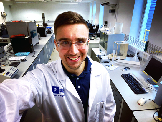
Dr Zakhar Kudrynskyi is a Research Fellow at the Faculty of Engineering, the University of Nottingham, UK. He studied at Chernivtsi National University in Ukraine where he graduated with first-class honours in Computer Engineering in 2010. Following that, he obtained his PhD in Physics of Semiconductors and Dielectrics at the Institute for Problems of Materials Science, National Academy of Sciences of Ukraine, Chernivtsi, Ukraine, in 2014. After his PhD, Dr Kudrynskyi worked abroad and in the School of Physics and Astronomy at the University of Nottingham, UK. In 2020 he joined the Advanced Materials Research group in the Faculty of Engineering at Nottingham. Currently, his main interests involve the science and technologies of innovative thin-film coating materials for electrical machines, power electronics, aerospace and renewable energy sectors.
1. Please summarize the research you do and explain why it is significant.
My current research is focused on the development of a novel class of high-performance, purely inorganic, electrically insulating materials designed using the concept of multi-layered thin films. These materials exploit the high thermal conductivity and dielectric strength of selected ceramic compounds, such as metal nitrides, to deliver a step change in the existing electrical and thermal limits in operational conditions: namely permitting continuous operation with high thermal conductivity at high temperatures ≥ 600°C and voltages ≥ 1.5 kV AC/DC, far beyond the capabilities of any existing electrical insulation.
2. How might your research be used?
This research aims to develop a radical innovation in electrification technologies previously infeasible with present electrically insulating coatings and manufacturing methods. My long-term ambition is to bring these coating materials from laboratories to everyday use, where they can really make a difference in a wide range of technologies, e.g., renewable energy, electric vehicles, hybrid aircraft (hydrogen/fully electric), industrial drives, robotics, low-carbon maritime and rail, offering innovative solutions to global challenges. This will be a vital step towards replacing fossil fuels with renewable powers to manage climate change and aligns with the UK government's ambitious target to reduce all greenhouse gas emissions to net-zero by 2050.
3. Why is the Park AFM important for your research?
The Park Systems NX20 large sample AFM equipped with high voltage tool kit and temperature controlled stage has been used in this research. This Park AFM enables different types of characterization of the surface of the ceramic thin films including: i) topographical characterization of the surface; ii) conductive atomic force microscopy measurements of leakage current and breakdown voltage at nanoscale; iii) determination of nanomechanical properties. The system offers a unique opportunity to combine all these measurements within a single piece of equipment and enables a significant acceleration of experimental measurements and high reproducibility of the obtained results.
4. What features of Park AFM are the most beneficial and why?
The NX20 is a state-of-the-art AFM combining unprecedented ease of use with a whole range of advanced imaging modes built into a single software package. The low-noise high-voltage amplifier and high temperature tool kit are key to this research project which studies high dielectric breakdown field strength of magnetron sputtered AlN thin films. In particular, the temperature-controlled stage enables to conduct measurements in a wide temperature range, namely from ambient temperature to 250 °C. The low-noise high-voltage amplifier for NX enables the application of high voltage bias up to ±150V (20x amplification ratio) to the samples. The unique capability to perform high voltage dielectric breakdown measurements whilst heating the sample up to 250°C makes it a perfect tool for investigation of thin-film samples for the most demanding applications.
Felix Pertl was born and raised in Austria. He obtained a master’s degree in physics with a major in surface science and semiconductor physics from TU Graz, Austria. Now he moved to Vienna to pursue his Ph.D. at IST Austria. After 3 successful rotation projects spanning from quantum dots, superconductivity to contact electrification (CE), he joined the soft matter and complex materials group of Scott Waitukaitis. His research focuses on studying contact electrification with Kelvin Probe Force Microscopy. Outside the lab, he likes to play tennis, skiing, and hiking.
1. Please summarize the research you do and explain why it is significant.
Everyone has experienced walking across a rug and then being shocked when they touch a metallic surface. The transfer of charge that occurs with the rug is known as contact electrification (CE). Although CE is a ubiquitous and widely studied phenomenon, it is poorly understood. I study the patterns of charge that appear on a surface after CE using Kelvin Probe Force Microscopy. These insights at the nanoscale promise to shed light on this universal yet puzzling phenomenon.
2. How might your research be used?
Recently, I have developed a rigorous technique for how to convert KPFM potential maps into charge density maps. Previously, KPFM with insulators had mostly reported just the potential or extracted charge in an ad hoc way. With my technique, we can now quantitatively do CE experiments at the nanoscale.
3. Why is the Park AFM important for your research?
The workhorse driving my entire research project is the NX20. Without this device, we could not even dream of measuring the quantities we do.
4. What features of Park AFM are the most beneficial and why?
The single-pass mode combined with Powerscript is extremely useful for me. Not only is single-pass mode twice as fast as double-pass mode, but it also allows to record the KPFM potential signal without a lift step and therefore at closer proximity to the surface. Powerscript allows me to schedule multiple measurements to study time-dependent discharging events, allowing me to catch my breath.