


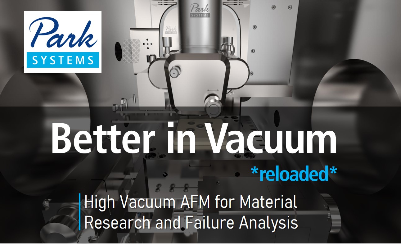
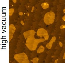
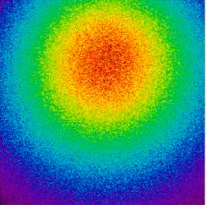
 高真空でナノスケール測定を実行すると、取得したデータの感度と分解能が大幅に向上し、材料分析力が強化されます。高真空環境では、周囲または乾燥N2環境よりも正確性と再現性の高いスキャンができるため、ユーザーは半導体材料お よび故障解析アプリケーションにおいて、幅広いドーパント濃度と信号応答の測定が可能です。高真空環境でのナノスケールAFM特性評価の優れた機能の詳細につきましては、「Better in Vacuum」ウェビナーシリーズ、最新のアプリケーション ノート、著名な研究ユーザーからの刺激的な研究結果をどうぞご覧ください。
ウェビナー
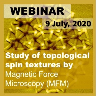
Thursday, July 9: Advanced high vacuum Magnetic Force Microscopy (MFM): study of topological spin textures
In this webinar, Dr. Karim Bouzehouane, CNRS Thales France, presents the capabilities of Magnetic Force Microscopy #MFM in high vacuum for studying of topological spin textures.
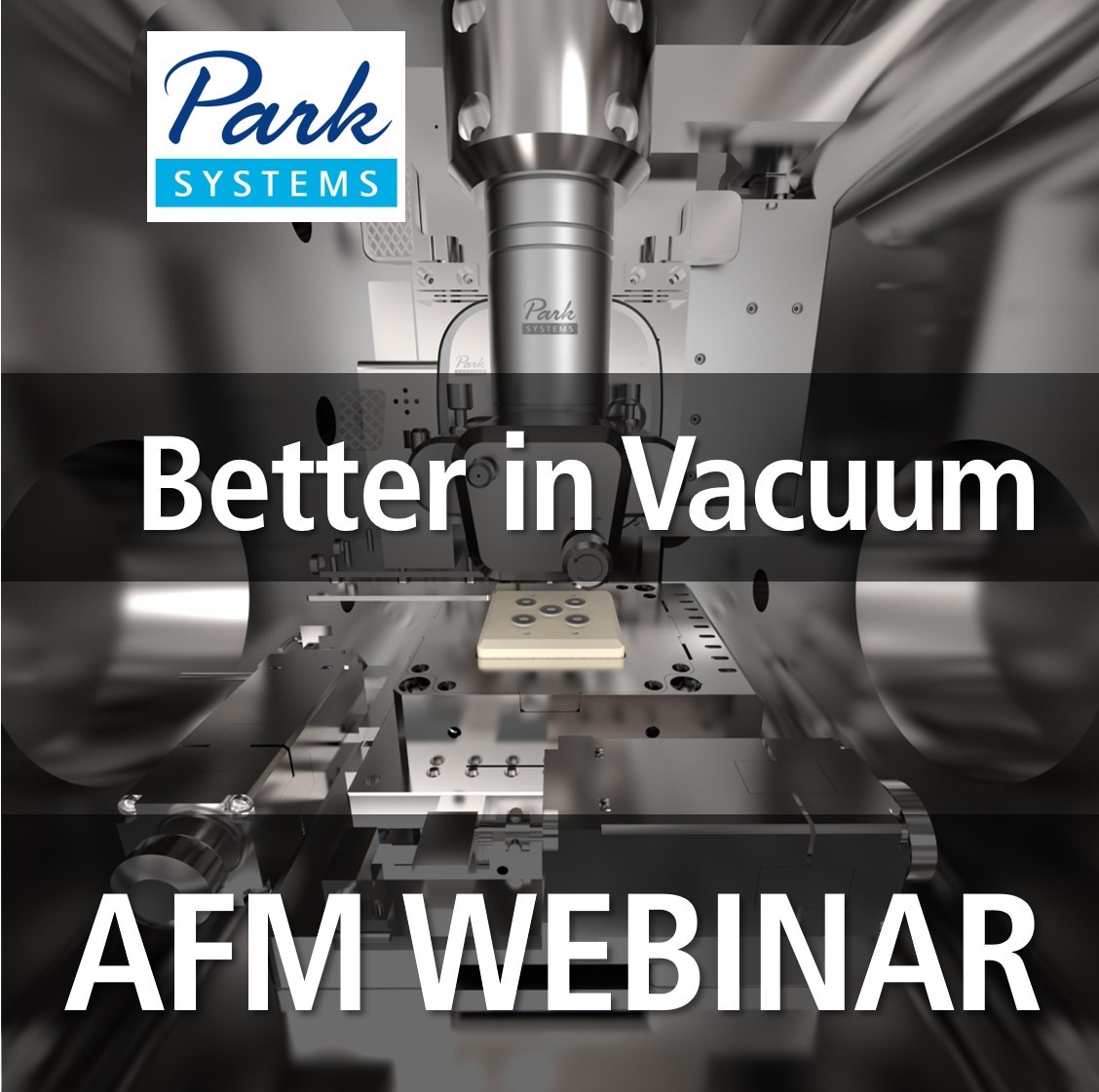
Thursday, 23 July: Better in Vacuum – how high vacuum improves the accuracy of nanoscale AFM characterization (on NX-Hivac AFM)
The webinar will give a full introduction to the high vacuum AFM functions and will show the easy-to-use pumping station interface. Moreover, some test measurements will be performed in Frequency Modulation AFM.
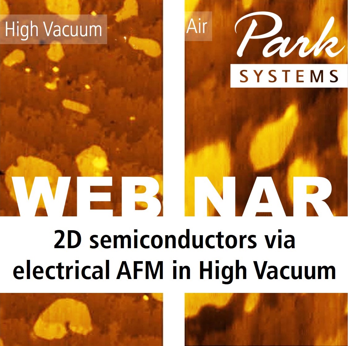
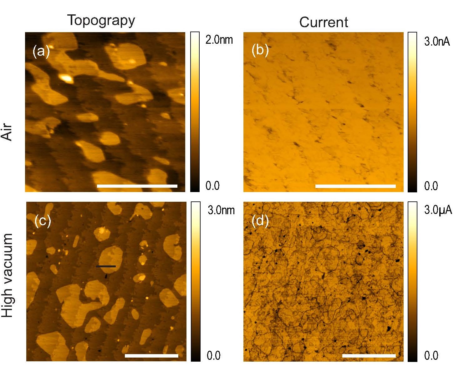
Thursday, 3 September: Better in Vacuum – boosting the characterization of 2D semiconductors via electrical AFM in high vacuum
In this webinar, we will demonstrate on Park’s NX Hivac how high vacuum (10-5 Torr) significantly improves the sensitivity and the resolution of electrical AFM modes on TMDs.
ソリューション
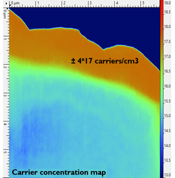
Pushing the sub 10 nm nodes device characterization with high vacuum SSRM providing the highest spatial resolution and high vacuum SCM improving carrier type sensitivity.
Read the app note: Carrier profiling in high vacuum using Scanning Spreading Resistance Microscopy and Scanning Capacitance Microscopy
Investigating 2D materials: the advantages of high vacuum for electrical measurements utilizing the capabilities of the Park NX-Hivac atomic AFM using MoS2 as an example material.
Read the app note: Advantages of high vacuum for Electrical Scanning Probe Microscopy
Understanding the electrical and mechanical properties of Lithium ion batteries (LIBs) for modern battery applications by using PinPoint™ Scanning Spreading Resistance Microscopy
Read the app note: Electrical and Mechanical Characterization of Li Ion Battery Electrode using Pinpoint SSRM
Performing scanning spreading resistance microscopy (SSRM) and conductive AFM (C-AFM) in high vacuum significantly improves accuracy, repeatability and homogeneity of data.
Read the technical note: Better in Vacuum: on the advantages of High Vacuum environment for Electrical Atomic Force Microscopy
出版物
Nanoscale Localization of an Atom Probe Tip through Electric Field Mapping I Read the paper
In this paper researchers propose a novel method to measure atom probe tomography (APT) specimen in three dimensions without damaging the SPM probe or specimen. The Electrostatic Force Microscopy (EFM), performed on Park NX-Hivac #AFM, is free of any mechanical interaction between both tips prior to surface imaging and is applicable for all possible probe geometries. The study is promising for further development of experimentally probing the 3D electric field distribution around an APT tip.
インタビュー
Rising Star of High Vacuum AFM and the AFM Scholarship Winner, Dr. Yuanyuan Shi

Dr. Yuanyuan Shi is a Postdoctoral fellow (Funded by Marie Curie Fellowship from European Commission) at IMEC, Belgium. Her expertise spans the development of wafer-scale two-dimensional (2D) materials based on transistor technology for scaling high-performance logic devices beyond 3 nm technology node.
Dr. Shi published over 50 scientific papers, she is an active reviewer for i.a. Nature, Nature Electronics, IEEE Electron Device Letters, and she is a member in IEEE EDS Nanotechnology committee. She has been recognized as a Forbes 30 under 30 (one of the world’s most impactful community of young entrepreneurs and game-changers) in 2020 and also as one of the Rising Stars Women in Engineering in 2018.
What is the impact of your research:“We are making efforts to achieve wafer-scale, uniform and single-crystalline growth of 2D materials, wafer-scale and clean transfer of 2D materials, and improvements to solve the specific issues (contact resistance, gate stacks, variability, reliability, yield, etc.) for large-area integration of 2D materials based nanoelectronics. Our research work will pave the way to large-area integration and industrialization of 2D materials-based transistors for beyond 3 nm technology node.”
Read the full interview.