


-
PvdfFilm PyroelectricDetector Bmp HiVacuum MechanicalProperties LightEmiting StyreneBeads Microchannel sputter mono_layer Sio2 Growth HexagonalBoronNitride CntFilm Dimethicone Morphology layers CastIron vertical_PFM ScanningKelvinProbeMicroscopy Conductivity Indent Strontium Tungsten Sperm Epoxy Filter PinPointMode BiVO4 FAPbI3 FuelCell Melt Vortex MagneticPhase SicMosfet
Report image
If you found this image unacceptable, please let us know. We will review your report and take action if we determine this image is really unacceptable.
Trench Etch Profile on Si Wafer
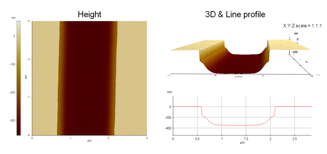
Top dielectric trench etch profile on Si wafer having tapered slope at the trench sidewall.
Scanning Conditions
- System: NX20
- Scan Mode: Non-contact
- Cantilever: AC160TS (k=26N/m, f=300kHz)
- Scan Size: 3μm×3μm
- Scan Rate: 0.21Hz
- Pixel: 1024 × 256
- Scan Mode: Non-contact
- Cantilever: AC160TS (k=26N/m, f=300kHz)
- Scan Size: 3μm×3μm
- Scan Rate: 0.21Hz
- Pixel: 1024 × 256