


-
CntFilm Solar DOE AM_SKPM light_emitting PVAC piezoelectric force microscopy domain_switching mechanical property plastics Electronics CuSubstrate AAO molecular_beam SelfAssembly Defect Chemical Vapor Deposition Chungnam_National_University ito_film Collagen LateralPFM SurfaceChange Conductivity PetruPoni Indium_tin_oxide Tape Nanofiber NiFe HexagonalBoronNitride Annealed STO PtfeFilter CeNSE_IISc BlockCopolymer PrCurve
Report image
If you found this image unacceptable, please let us know. We will review your report and take action if we determine this image is really unacceptable.
MoS2 Layers on SiO2
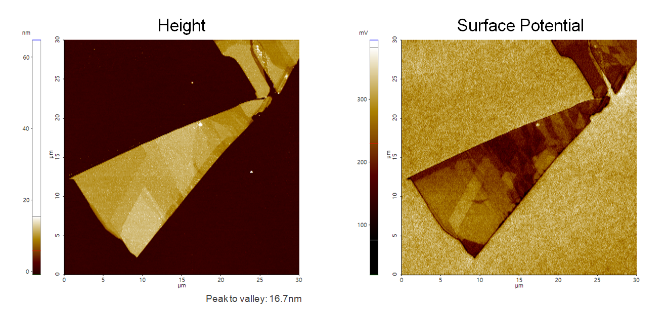
A few layers of MoS2 on SiO2
Scanning Conditions
- System: NX10
- Scan Mode: AM-KPFM
- Cantilever: NSC36Cr-Au B (k=2N/m, f=130kHz)
- Scan Size: 30μm×30μm
- Scan Rate: 0.3Hz
- Pixel Size: 512 × 256
- Scan Mode: AM-KPFM
- Cantilever: NSC36Cr-Au B (k=2N/m, f=130kHz)
- Scan Size: 30μm×30μm
- Scan Rate: 0.3Hz
- Pixel Size: 512 × 256