


-
CompactDisk Filter Mapping 2d_materials SPMLabs SICM HafniumDioxide STM Protein #EC PetruPoni Optical PDMS PhaseTransition MultiferroicMaterials Phosphide Copolymer Hair TappingMode Kevlar Moire Resistance PolyStylene Bmp Polyvinylidene Korea nanomechanical norganic Terrace Topography DLaTGS Graphene AEAPDES Sio2 Writing
Report image
If you found this image unacceptable, please let us know. We will review your report and take action if we determine this image is really unacceptable.
Taegeuk Mark Lithography on PZT
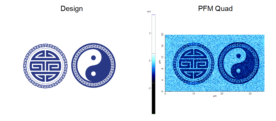
Re-arranged the domain pole direction on PZT surface using bias mode of lithography.
Scanning Conditions
- System: NX10
- Scan Mode: Lithography
- Cantilever: PPP-ContScPt (k=0.2N/m, f=25kHz)
- Scan Size: 35μm×20μm
- Scan Rate: 0.5Hz
- Pixel Size: 1024 × 1024
- Tip Bias: 10V for patterned area
- Scan Mode: Lithography
- Cantilever: PPP-ContScPt (k=0.2N/m, f=25kHz)
- Scan Size: 35μm×20μm
- Scan Rate: 0.5Hz
- Pixel Size: 1024 × 1024
- Tip Bias: 10V for patterned area