


-
LeakageCurrent SiWafer Pinpoint NCM\ temperature controller AFM Pattern FrictionalForce Topography Wafer GlassTemp AM_SKPM HafniumDioxide Barium_titanate Vinylpyridine LateralPFM LithiumNiobate semifluorinated alkane Aluminium_Oxide Magnetostrictive OpticalElement ScratchMode Film electrospinning Holes Sulfur FFM Microchannel INSP Optoelectonics Layer MechanicalProperty ItoGlass TungstenDeposition high_resolution HBN
Report image
If you found this image unacceptable, please let us know. We will review your report and take action if we determine this image is really unacceptable.
Nanostructures on polymer
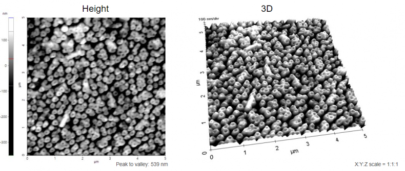
Scanning Conditions
- System : NX10
- Scan Mode: Non-contact
- Scan Rate : 0.5 Hz
- Scan Size : 5μm×5μm
- Pixel Size : 256×256
- Cantilever : PPP-NCHR (k=42N/m, f=330kHz)