


-
Polyethylene HfO2 epitaxy ULCA Defects Fiber Water Pattern Film Foil Multiferroic_materials temp_control DIWafer IMT_Bucharest Heating Scanning_Thermal_Microscopy self_assembly Sadowski dielectric_trench Steps electrospinning LightEmiting Electrode Battery temperature controller AFM semifluorinated_alkanes Conductance Bacterium Cancer Polyurethane cross section HiVacuum Change BTO Semiconductor
Report image
If you found this image unacceptable, please let us know. We will review your report and take action if we determine this image is really unacceptable.
Semiconductor device, Failure analysis
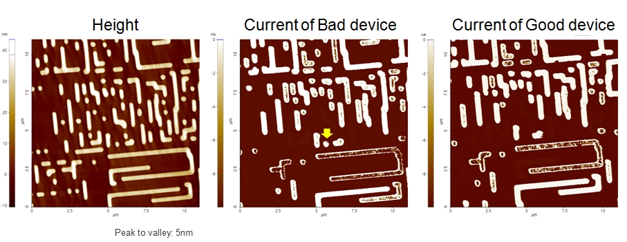
Scanning Conditions
- System: NX10
- Scan Mode: Conductive AFM
- Cantilever: CDT-Contr (k=0.5N/m, f=20kHz)
- Scan Size: 11μm×11μm
- Scan Rate: 1Hz
- Pixel: 512×512
- Sample bias: -0.5V