


MoS₂


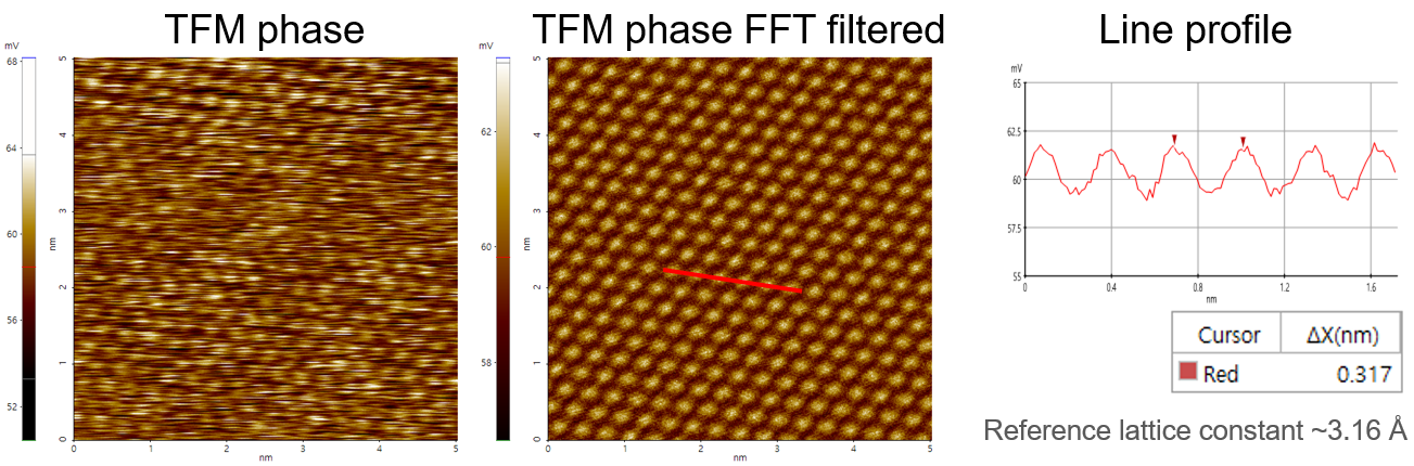
MoS₂ is a layered two-dimensional semiconductor with a well-defined hexagonal in-plane lattice structure (~3.16 Å).
TFM phase imaging over a 5 nm × 5 nm area resolved the atomic lattice, and FFT filtering with line-profile analysis confirmed a periodic spacing of ~0.316 nm, consistent with the known lattice constant.
Scan Conditions
- System: NX1
- Scan Mode: TFM
- Scan Size: 5 nm×5 nm
- Scan Rate: 15 Hz
- Pixels: 360×360
- Cantilever: SCOUT 70
(k=2 N/m, f=70 kHz)


×