


James Kerfoot1
1Park Systems UK Ltd, Medicity nottingham, D6 Building Thane Road, NG90 6BH, UK
Introduction
Layered materials heterostructures (LMHs) [1] consist of vertically stacked flakes of layered materials (LMs), which are widely utilised for reasons including enabling LM flakes with properties closer to their intrinsic limit [2], the formation of sophisticated device architectures [3] and controlling layer registries deterministically [4]. AFM is an important tool to track and assist the fabrication of LMHs and their devices since, in addition to verifying layer thicknesses, it can be used to perform tasks such as cleaning interfaces, cutting layers both mechanically and via anodic oxidation and confirming the alignment of buried layers.
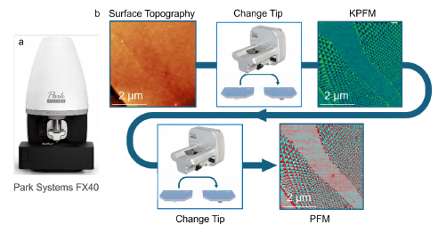
Figure 1. The Park FX40 automatic AFM is shown (a) as well as a schematic illustrating the ability of the FX series to change probes for different modes and functions (b), with topography, KPFM potential and PFM phase images acquired from parallel stacked hBN on graphene.
In this application note, we present Park Systems’ FX series products as ideal tools to monitor and improve the formation of layered materials heterostructures with three examples. In our first example, we show how performing in-situ contact mode cleaning [5-8] at elevated temperatures leads to cleaner interfaces that exhibit moiré patterns. In the second part, we show how anodic oxidation can be used to controllably cut graphene, including over extended areas. Our final example shows how patterns cut into graphene can be incorporated into vertical heterostructures and the alignment of the buried flake within the heterostructure tracked using electrical AFM.
Results and Disscusion
Our first example is AFM cleaning, a process that utilises contact mode AFM. In this mode, the feedback of the AFM probe monitors the vertical deflection of the cantilever. As such, a force is applied in the out-of-plane direction between the surface and tip of the probe which can be controlled by changing the setpoint. Since the feedback loop in AFM maintains the setpoint, a controlled vertical force is applied uniformly across the substrate, which promotes the removal of contaminants from both the top surface and buried interfaces of LMHs. Such AFM cleaning experiments have been convincingly shown to improve the performance of LMH devices [6] and sharpen the linewidths of photoluminescence from transition metal dichalcogenide monolayers [5, 8].
Here, we present a commercially available solution in which we perform AFM cleaning on our FX series instruments with an in-situ heating stage, as shown in figure 1. To demonstrate the applicability of this technique, an MoS2 homostructure formed by partially transferring, tearing and stacking of a monolayer (1L-)MoS2 flake (~0.7 nm thickness) on highly oriented pyrolytic graphite (HOPG) with a ~0˚ twist angle was prepared [9] using a polydimethylsiloxane (PDMS) stamp[10]. Viscoelastic stamping with PDMS is a very convenient and versatile technique for heterostructure fabrication, but residues from the PDMS can contaminate both the top surface and buried interfaces [11], which motivates the use of cleaner but more laborious techniques [12, 13]. In the fabrication method used here, PDMS was in contact with the top surface of the bottom MoS2 flake prior to completion of the sample, yielding contaminated interface, as seen in the AFM height image of the sample before cleaning (see figure 2b).
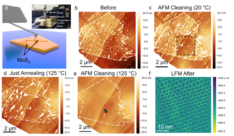
Figure 2. Cleaning buried interfaces may be performed with greater efficacy by using contact mode AFM (a), with a heating stage (inset a). A starting homostructure consisting of a mechanically torn and stacked MoS2 flake (of ~0.7 nm thickness, determined by AFM topography after cleaning) was measured using NCM mode with an NCHR probe (b), revealing a high degree of buried interfacial contamination, seen as areas of higher topography. AFM cleaning was then performed using an LFMR probe with a setpoint of ~20 nN over a 3 μm area indicated by a dashed black box overlaid on a scan of the whole flake acquired in non-contact mode (c). Upon annealing to 125 °C, the buried contamination was found to aggregate into larger blisters (d) which were completely removed upon performing contact mode cleaning (again with ~20 nN force) at 125 °C (e). The quality of the resulting cleaned interfaces was confirmed by LFM images showing a clear moiré pattern (f).
After an initial reference scan to determine the morphology of trapped contaminants using non-contact mode (NCM), a room temperature contact mode cleaning step was performed over a 3 μm region of the restacked MoS2 (see figure 2c), revealing a partial cleaning effect. Raising the temperature of the stage to 125 °C led to the aggregation of blisters (see figure 2d). Upon the completion of AFM cleaning at 125 °C, the whole MoS2 homostructure was found to be cleaned. The improved efficacy of performing the cleaning in-situ is confirmed by comparing the results of cleaning at room temperature and only annealing (see figures 2 c and d respectively) in addition to the observation of a moiré pattern on the stacked and cleaned MoS2 bilayer, performed in lateral force microscopy (LFM) with a PPP-CONTSCR probe (k ~0.2 N/m), which would be suppressed by any interfacial contamination.
The efficacy of the combined annealing and AFM cleaning setup is encouraging since performing annealing via the sample stage and applying force via the tip simultaneously should improve the yield of the technique at lower forces and temperatures, which is particularly convenient for materials which are sensitive to temperature or easily damaged by the tip, InSe being a notable example. While the temperature control stage illustrated inset in figure 2a is incompatible with the automated tip exchange feature of the FX series, performing room temperature cleaning with our FX series instruments offers the opportunity to automatically switch between different types of probes, such that a sharp tip mounted on a lever suited to non-contact mode experiments could be used to check the morphology before versus after cleaning, while a probe with a soft lever could be used for cleaning steps.
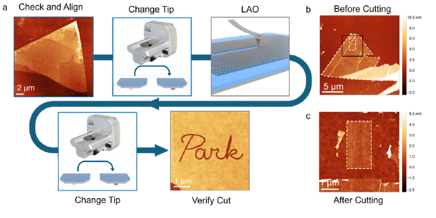
Figure 3. The anodic oxidation of few-layered graphene performed using Park Systems’ FX series AFMs. The workflow of such an experiment (a) consists of a reference scan to check the morphology and cleanliness of a flake before the system exchanges to a conductive probe (in this case an AD2.8AS) for the anodicoxidation step. After the anodic oxidation is performed, the system can then be used to switch back to the original probe used to measure the surface topography. In addition to cutting lines, cutting can also be performed over extended areas to remove several square μm of material. Panels b and c show the surface topography of a few-layered graphene flake before and after the removal of large areas.
In our second example, we show the anodic oxidation of few layer graphene (FLG) [14, 15], a technique that applies an AC voltage(VAC) to a conductive AFM probe to etch graphene due to electrochemical reactions within the water meniscus at the tip-sample junction. In figure 3a, we show the workflow for anodic oxidation of graphene (as described in our earlier application note [16]), where a VAC of 8 V at 40 kHz is applied to an AD2.8AS probe with a humidity of >60%. Cutting from the edge of graphene flakes on SiO2 is easily achieved by scanning with lateral speeds of ~1 μm/s. Cuts from the centre of flakes are typically more challenging, as applying VAC to the tip already in electrical and mechanical contact with an LM flake does not yield conditions that generate cutting. Instead, cuts from the centre of flakes are initiated via very slow (~10 nm/s) approach speeds. As exemplified by figure 3a, our SmartLitho package supports the formation of detailed and user defined patterns into graphene flakes via anodic oxidation. In addition to cuts due to a single pass of the AFM probe, larger areas of graphene can be selectively etched by scanning the probe across the surface, as shown in figure 3b and c, where a 1.5 x 3 μm pad is isolated from a much larger FLG flake.
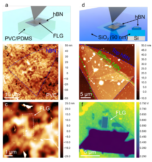
Figure 4. The incorporation of features cut by AFM based anodic oxidation and the measurement of buried features by electrical AFM. A schematic of the FLG/hBN heterostructure on a PVC film on PDMS is shown (a), in addition to AFM topography (b and c) depicting the alignment of the FLG and hBN flakes (b) and a smaller field-of-view image of the 1.5 x 3 μm FLG pad that had been picked up (c). By picking up a second hBN flake, the FLG pad was hBN encapsulated before being transferred onto a fresh Si + 90 nm SiO2 substrate, with an AFM image of the completed heterostructure shown (e). The FLG pad, indicated by a white dashed line and very faint in the topography image (e) was measured using lift-mode KPFM, with the outline of the FLG pad shown clearly in the contact potential difference map (f).
An important feature in using AFM to deterministically etch graphene for LMH devices is the ability to check the results of cutting while keeping the humidity of the enclosure constant. This ensures the enclosure humidity is stable while further steps are performed to correct any errors or to monitor the width of the etched features (which can depend upon the condition of the probe). In this regard, Park Systems’ FX series instruments are ideal since their probe exchange capacity enables the automatic exchange between sharp probes used to check flakes before/after oxidation and even swap between different conductive probes so that sharper probes are saved to use for features that need to be very fine (<50 nm), all without needing to open the enclosure to change the probe, which could affect humidity or thermal drift and reduce the yield of the process.
One key aspect of AFM based anodic oxidation of graphene is the ability to incorporate patterned features into more sophisticated structures, for example to act as a gate in a field effect transistor. In figure 4a-c, we show the rectangular FLG pad shown in figure 3c after picking up with a hBN with a stamp used for dry transfer of LMs [17]. The stamp was prepared by stretching a PVC film over a PDMS block on a glass slide. The stamp was then aligned to a hBN flake on Si + 90 nm SiO2 identified by optical microscopy and brought into contact and retracted at 60 °C using a micromanipulator stage to pick the flake up. The hBN flake on the PVC stamp was then aligned to the FLG pad and picked up (also at 60 °C). AFM topography measurements were performed on the FLG/hBN on PVC film to verify that the pad was successfully picked up and was free from contamination (background roughness arises from the PVC film itself).
In our final example, we also show how electrical AFM can be used to measure the position of buried flakes that may be difficult to measure in topography due to their low relative thickness compared to encapsulating flakes or in optical microscopy due to interference effects. In figure 4 panels d and e, we show a schematic and AFM image of the 1.5 x 3 μm FLG pad that is now fully encapsulated in hBN (top hBN: ~13.1 nm thick and bottom hBN: ~9.9 nm thick) and transferred to a new Si + 90 nm SiO2 substrate. The encapsulation and transfer were performed by picking up a second hBN flake at 60°C before transferring the completed stack from PVC onto a clean Si + 90 nm SiO2 surface at 150 °C. In order to visualise the SLG (single layer graphene) pad, we performed lift-mode Kelvin probe force microscopy (KPFM) with a 20 nm lift height and an electrical excitation (VAC = 2 V) applied at the 2nd eigenmode of the cantilever.[18] The 2nd eigenmode was chosen as it offers increased sensitivity versus off-resonance techniques while being less surface specific than techniques such as heterodyne (HD-) and sideband (SB-) KPFM [19], thus enabling contrast from buried features. Such a KPFM image is shown in figure 4f and clearly shows the outline of the patterned FLG pad buried under ~13.1 nm of hBN. These results demonstrate that it is possible to verify the alignment of buried flakes within LMHs that are not easily identifiable via optical microscopy or in AFM topography.
Conclusion
In conclusion, we highlight how Park Systems’ FX series AFMs can augment the fabrication of LMHs. We first show how performing AFM cleaning experiments with in-situ heating enables interfacial contamination to be removed with near 100 % yield, which holds great promise for improving the ease of implementation, efficacy and range of operating conditions (both in terms of temperature and mechanical setpoint) of AFM cleaning. We then showcase the use of anodic oxidation to pattern LMs with narrow cuts formed by one pass of the probe and also over larger areas, with applications including cutting flakes to stack them with controlled twist angle and resist-free patterning. We then demonstrate how flakes patterned by anodic oxidation can be incorporated into LMHs and use AFM both to track the cleanliness of interfaces during heterostructure assembly and to measure buried interfaces within completed LMHs using electrical AFM.
References
- A. Geim and I. Grigorieva, Nature 499, 419–425 (2013)
- C. Dean et al. Nature Nanotech 5, 722–726 (2010)
- F. Withers et al. Nature Mater 14, 301–306 (2015)
- R. Ribeiro-Palau et al. Science 361,690-693 (2018)
- M. Rosenberger et al. ACS Appl. Mater. Interfaces 10, 12, 10379–10387 (2018)
- Y. Kim et al. ACS Nano 13, 12, 14182–14190 (2019)
- D. G. Kim, S. Lee and K. Kim. Appl. Microsc. 50, 28 (2020)
- S. Chen et al. ACS Omega 6, 5, 4013–4021(2021)
- K. Kim et al. Nano Lett. 16, 3, 1989–1995 (2016)
- A. Castellanos-Gomez et. al. 2D Mater. 1 011002 (2014)
- A. Jain et al. Nanotechnology 29 265203 (2018)
- F. Pizzocchero et al. Nat Commun 7, 11894 (2016)
- D. G. Purdie et al. Nat Commun 9, 5387 (2018)
- J. Yu, et al. Adv. Mater. Interfaces 12, no. 16 (2025): 12, 2500137
- Hongyuan Li et al. Nano Letters 2018 18 (12), 8011-8015
- R. Nguyen et al. Nanopatterning on 2D materials by AFM-based nanolithography
- Y. Wakafuji et al. Nano Letters 2020 20 (4), 2486-2492
- Maria J Cadena et al 2018 Nanotechnology 29 405702
- A. Axt et al. Beilstein J. Nanotechnol. 2018, 9, 1809–1819
