


Dr. Kalaiarasan Meganathan is a Postdoctoral Researcher in the Sofer Group at the University of Chemistry and Technology, Prague, specializing in the synthesis and nanoscale characterization of two-dimensional materials. Building on his doctoral research on the thickness dependent nanomechanics of atomically thin MoS₂, his work now focuses on scalable CVD/MOCVD growth, AFM-based characterization, strain engineering, and translating 2D materials toward advanced sensing, flexible electronics, and optoelectronic applications.
1. Please summarize the research you do and explain why it is significant?
My research focuses on the synthesis and nanoscale characterization of two dimensional transition metal dichalcogenides, particularly atomically thin MoS₂. I grow these materials by gas-phase chemical vapor deposition / metal-organic chemical vapor deposition (MOCVD), and I study how layer thickness, strain, defects, and growth conditions influence their mechanical, structural, and optical properties.
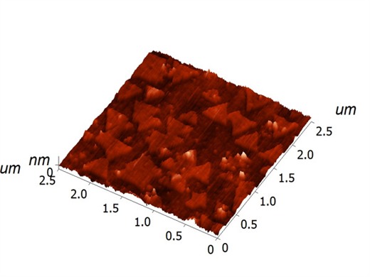
A central part of my doctoral research was the thickness dependent nanomechanics of MOCVD-grown MoS2. I combined atomic force microscopy (AFM) with atomic force acoustic microscopy (AFAM), a contact-resonance technique, to measure local elastic properties without the need to fabricate suspended membranes. Across films from approximately 0.75 to 15 nm thick, I observed a pronounced reduction in Young's modulus from about 273 GPa for the thinnest material to about 102 GPa at larger thickness, following an inverse thickness dependence close to t⁻¹·¹⁶. I correlated these nanoscale measurements with Raman and photoluminescence spectroscopy, electron microscopy, XPS, analytical mechanics, and density-functional-theory calculations.
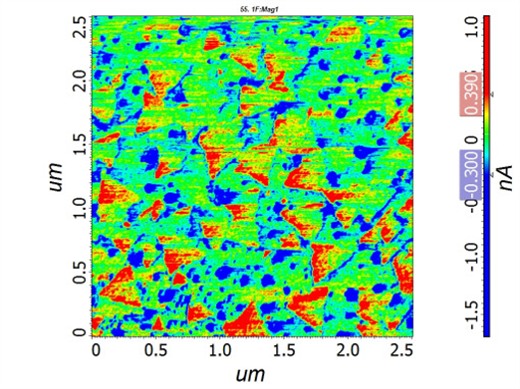
This is significant because an atomically thin material cannot always be treated as a scaled-down bulk crystal. Adding only a few layers can change its stiffness, bending resistance, interlayer sliding, strain distribution, and ultimately its electronic and optical response. Establishing these thickness dependent mechanical limits is therefore important for designing reliable 2D material devices rather than assuming a single bulk mechanical property.
2. How might your research be used?
The immediate use of this research is to provide practical mechanical design rules for 2D material devices, especially in flexible electronics. Knowing how Young's modulus, bending rigidity, strain energy, and buckling behavior evolve with thickness helps researchers choose the appropriate number of layers for flexible electronics, strain-engineered optoelectronics, sensors, and nanoelectromechanical systems.
For example, very thin MoS2 can tolerate bending and conform to flexible substrates, while thicker films progressively behave more like a rigid layered solid. By combining these mechanical measurements with Raman and photoluminescence studies under externally applied strain, my work also helps identify how mechanical deformation modifies phonons, excitons, trions, doping, and light emission. This is directly relevant to strain-tunable photodetectors, transistors, flexible sensors, and other devices in which mechanical deformation is not merely a reliability issue but can be used as a functional control parameter.
More broadly, my current work on scalable MOCVD/CVD growth of MoS2, WS2, related alloys, and other 2D systems aims to connect synthesis conditions with morphology and functional performance. The long-term goal is to move from isolated laboratory flakes toward reproducible, wafer-relevant materials whose growth, mechanical reliability, and device response can all be quantitatively engineered.
3. Why is the Park AFM important for your research?
AFM is important because the key questions in my research occur at length scales where conventional optical characterization is not sufficient. For atomically thin MoS2, I need to determine nanoscale thickness, surface morphology, roughness, local heterogeneity, and mechanical response with high spatial and vertical resolution. AFM allows me to identify these features directly and then correlate them with Raman, photoluminescence, and other measurements.
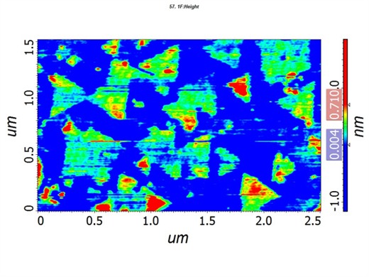
More importantly, the AFM platform enables my AFAM measurements. In AFAM, the sample is acoustically excited while the cantilever is in controlled contact with the surface, shifts in the cantilever contact-resonance frequency are used to determine local stiffness and Young's modulus. I used this approach, including the higher (2nd Order) contact-resonance response, to map elastic behavior across MoS2 films of different thicknesses. This made it possible to measure the mechanical evolution of supported ultrathin films locally and more important nondestructively, rather than relying only on suspended membrane indentation.
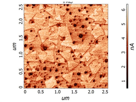
For my work, the AFM is therefore not simply an imaging instrument. It is the measurement platform that connects morphology, thickness, and nanoscale mechanics. Without that correlation, the central conclusion of my research is “nanoscale size effect”, i.e., elastic behavior of MoS2 changes strongly with thickness. It would be much more difficult to establish with the same spatial resolution and confidence.
4. What features of Park AFM are the most beneficial and why?
Several features are particularly valuable for my research. First, the high resolution, low-noise scanner and precise Z control are essential when the relevant height differences can be on the order of a single MoS2 layer (~ 0.65 nm). Accurate topography is important because even a small error in thickness assignment would directly affect the interpretation of thickness dependent mechanical properties.
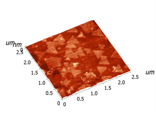
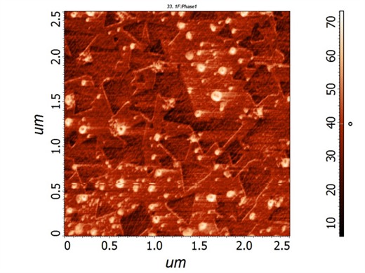
Second, Park's True Non-Contact™ imaging capability is highly useful for delicate ultrathin films. Minimizing direct tip-sample interaction helps preserve both the sample surface and the probe while providing repeatable topographic measurements. This is especially valuable when the same small region must later be compared with spectroscopic or mechanical measurements.
Third, the mechanical stability and repeatability of the AFM platform are critical for contact-resonance/AFAM measurements. In my work, relatively small changes in resonance frequency must be converted into meaningful differences in contact stiffness and Young's modulus. Stable force control, precise positioning, and reproducible scanning therefore directly improve the reliability of the mechanical maps and thickness dependent trends.
Finally, I value the ability to use the AFM as a multimodal research platform rather than only as a topography tool. For 2D materials, the most useful information often comes from correlating surface morphology with local mechanical, electrical, or other functional properties. That combination makes the Park AFM especially powerful for studying how nanoscale structure translates into device-relevant behavior.
%20Webinar.png)

