


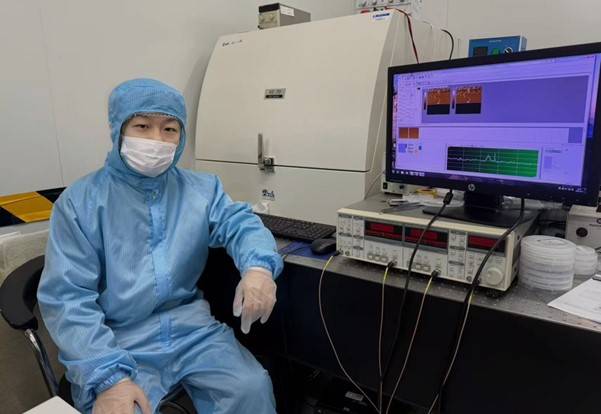
In the 2025 Park AFM Scholarship selection, Dr. Yao Yixu, Assistant Researcher from Prof. Jingyuan Shi’s research group at the Institute of Microelectronics, Chinese Academy of Sciences (IMECAS), was awarded the scholarship in recognition of his major breakthroughs in GaN defect physics.
His research, entitled “Dislocation-Assisted Electron and Hole Transport in GaN Epitaxial Layers,” was published in Nature Communications (DOI: 10.1038/s41467-025-61510-w). This work provides the first direct experimental evidence revealing the fundamentally opposite roles of threading screw dislocations (TSDs) and threading edge dislocations (TEDs) in carrier transport, thereby resolving a long-standing controversy in the field.
The study suggests that by engineering the relative densities of screw and edge dislocations during epitaxial growth, it is possible to achieve an optimal balance between leakage current and dynamic reliability in GaN power devices without compromising overall crystal quality. This breakthrough opens a new avenue for defect engineering in GaN devices, innovatively proposing that dislocations can be regarded as engineerable one-dimensional carrier transport channels, rather than purely detrimental structural defects.
This concept is expected to be extendable to other semiconductor material systems and lays an important foundation for the emerging theoretical framework of “dislocation electronics.”
1. Please summarize the research you do and explain why it is significant?
My research focuses on the physics of defects in wide-bandgap semiconductors, specifically unraveling the complex carrier transport mechanisms in Gallium Nitride (GaN). In our recent work published in Nature Communications, we addressed a long-standing debate regarding dislocation conductivity. By fabricating GaN epitaxial layers with controlled dislocation types, we provided the first experimental evidence distinguishing the roles of Threading Screw Dislocations (TSDs) and Threading Edge Dislocations (TEDs). We discovered that TSDs act as detrimental leakage paths for electrons via open-core structures and localized shallow states (ETSD). Conversely, we found that TEDs unexpectedly play a beneficial role by facilitating vertical hole transport through defect states (ETED), which helps mitigate charge trapping and improves device reliability.
Significance:
This research is significant because it fundamentally shifts the paradigm of "defect engineering" in GaN. Previously, all dislocations were broadly considered harmful scattering centers. Our findings reveal a dual-path mechanism where different dislocations manage electron and hole flows separately. This understanding is critical for solving the notorious "current collapse" and dynamic on-resistance (RON) degradation issues in GaN power devices. It provides a precise physical model that allows device engineers to optimize epitaxial growth not just by reducing total defect density, but by balancing the ratio of TSDs to TEDs for superior performance.
2. How might your research be used?
Our research provides a direct roadmap for the next generation of robust GaN power electronics.
- Epitaxial Growth Optimization: Manufacturers can now tailor growth conditions (using AlN vs. GaN nucleation layers) to suppress harmful TSDs while retaining a sufficient density of TEDs to aid in hole redistribution and leakage suppression.
- Device Reliability Engineering: The identified transport models explain failure mechanisms under high-voltage stress. Engineers can use our "dual-path" transport model to design buffer layers that utilize TED-assisted hole transport to neutralize electron trapping, thereby stabilizing dynamic RON in high-frequency switching applications.
- Novel Device Architectures: Beyond GaN, the methodology we established for characterizing dislocation-specific transport can be extended to other emerging materials like SiC, Diamond, and Perovskites, potentially leading to a new class of "dislocation-enhanced" electronic devices.
3. What features of Park AFM are the most beneficial and why?
For this study, the multi-mode capability and high spatial resolution of the Park AFM were the most beneficial features.
- Precise Defect Identification: We relied on the system's superior topography imaging to distinguish between specific dislocation types based on their etch-pit geometries—identifying TSDs as large trapezoidal β-pits and TEDs as small triangular α-pits.
- In-situ Electrical Characterization (c-AFM & EFM): The ability to switch seamlessly between Topography, Conductive-AFM (c-AFM), and Electrostatic Force Microscopy (EFM) on the exact same nanoscale region was crucial. This allowed us to directly correlate the physical structure of a single dislocation with its electrical behavior.
- Measurement Sensitivity and Stability: The c-AFM mode offered the sensitivity required to detect picoampere-level leakage currents in highly insulating structures. Furthermore, the system allowed us to perform scans with the laser switched off to eliminate photoelectric interference, ensuring the integrity of our leakage current data.
4. Why is the Park AFM important for your research?
Park AFM served as the bridge between macroscopic device performance and microscopic defect physics in our research.
While Photoluminescence (PL) and Deep-level Transient Spectroscopy (DLTS) provided energy level data, they lacked spatial resolution. We needed to prove where the leakage and transport were occurring physically. Park AFM allowed us to:
1. Directly Visualize Leakage Paths: We utilized c-AFM to definitively prove that leakage current is concentrated at the core of TSDs (open-core pits) while TEDs remain electrically insulating for electrons.
2.Map Potential Landscapes: Using EFM, we mapped the electrostatic potential distribution around dislocations, revealing a ~1 V potential well induced by TSDs.
Without the Park AFM's (XE-70) ability to provide this spatially resolved electrical data, our conclusion—that TSDs and TEDs have distinct, opposing roles in carrier transport—would have remained a theoretical hypothesis rather than an experimentally proven fact. It was the decisive tool that validated our first-principles calculations and completed our physical model.
%20Webinar.png)

